Anti-reflection coating and optical element having such anti-reflection coating for image sensors

Inactive Publication Date: 2006-07-13
ASAHI KOGAKU KOGYO KK
View PDF5 Cites 104 Cited by
  • Summary
  • Abstract
  • Description
  • Claims
  • Application Information

AI Technical Summary

Benefits of technology

[0009] Accordingly, an object of the present invention is to provide an anti-reflection coating having excellent anti-reflection characteristics to a wide-inciden

Problems solved by technology

For instance, a single-layer anti-reflection coating is designed to have such thickness that an optical path difference between light reflected from a surface of the anti-reflection coating and light reflected from an interface between the anti-reflection coating and a lens is in an odd multiplication of half a wavelength, resulting in cancellation of these lights by interference.
However, for instance, the larger numerical aperture an objective lens of a camera has, the larger curvature it has, resulting in a large incident angle of light in a peripheral portion of the lens.
Accordingly, there is a large amount of reflected light in the peripheral portion of a lens, resulting in differences in the amount and color of transmitted light between the center and peripheral portions of the lens,

Method used


Image

  • Anti-reflection coating and optical element having such anti-reflection coating for image sensors
  • Anti-reflection coating and optical element having such anti-reflection coating for image sensors
  • Anti-reflection coating and optical element having such anti-reflection coating for image sensors

Examples


example 1

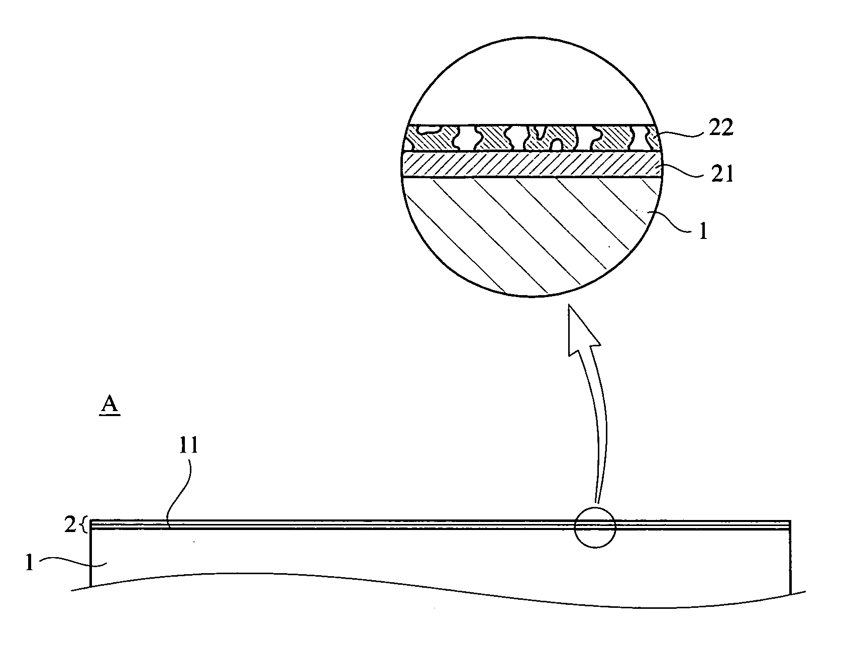
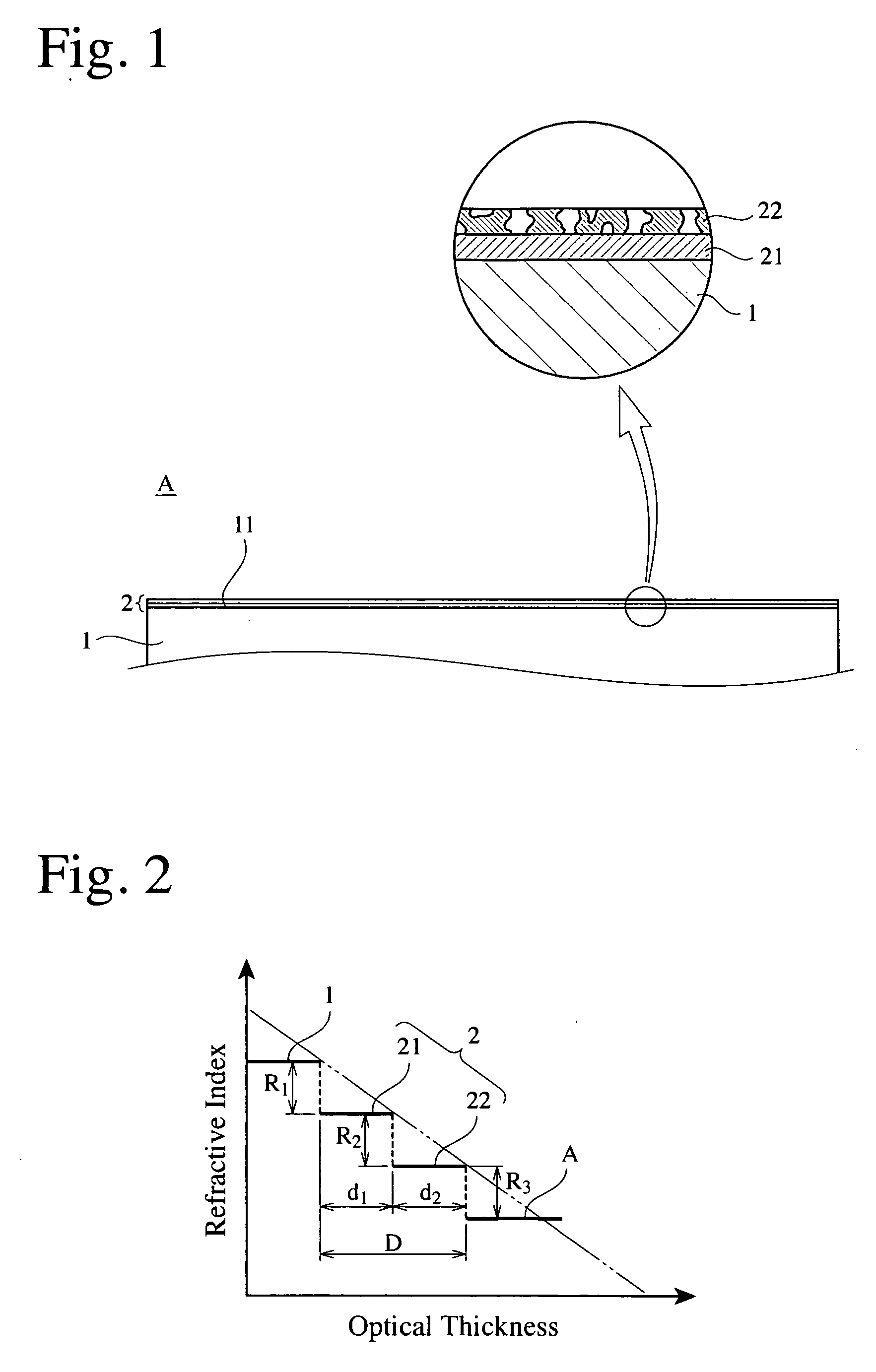
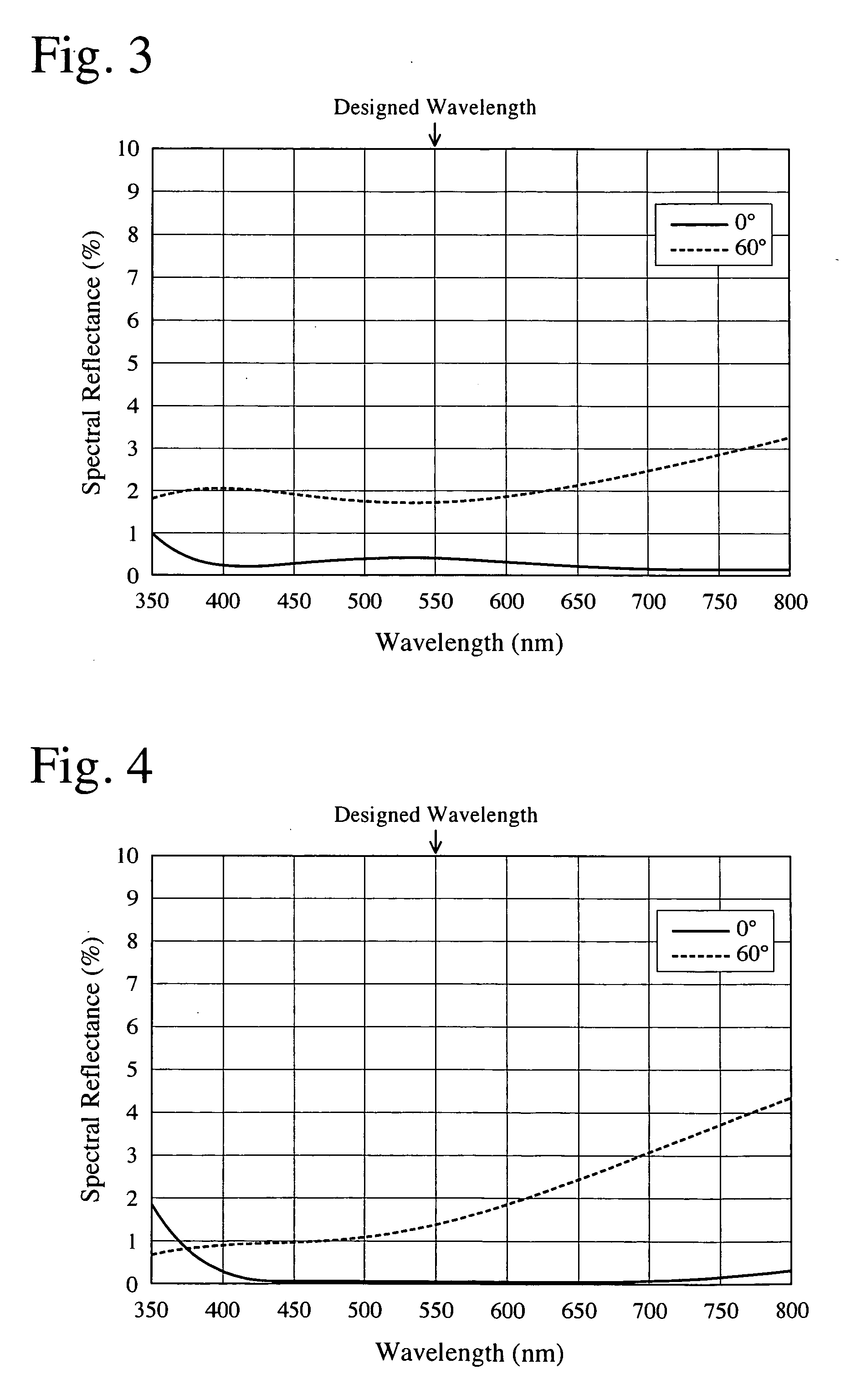
[0077] An anti-reflection coating was formed on a flat BK7 glass plate by the steps (1) and (2) below. The designed wavelength λd was 550 nm.

(1) Formation of Dense Layer

[0078] Using an apparatus with an electron-beam vapor deposition source, a magnesium fluoride layer (refractive index: 1.38) having a physical thickness of 94 nm (optical thickness: 130 nm) was formed on a flat BK7 glass plate having a refractive index of 1.518 at a wavelength of 550 nm by a vapor deposition method.

[0079] (2) Formation of Porous Layer

(i) Preparation of Organic-Modified-Silica-Containing Sol

[0080] After 5.21 g of tetraethoxysilane was mixed with 4.38 g of ethanol, 0.4 g of hydrochloric acid (0.01 N) was added thereto, and the resultant mixture was stirred for 90 minutes. After 44.3 g of ethanol and 0.5 g of an aqueous ammonia solution (0.02 N) were added, the resultant mixture was stirred for 46 hours. This mixed liquid was aged at 60° C. for 46 hours to form a wet gel. After decanting the solv...

example 2

[0083] A multi-layer anti-reflection coating was formed on a flat LAK14 glass plate by the steps (1) and (2) below. The designed wavelength λd was 550 nm.

(1) Formation of Dense Layer

[0084] Using an apparatus with an electron-beam vapor deposition source, a silicon oxide layer (refractive index: 1.46) having a physical thickness of 90 nm (optical thickness: 131 nm) was formed on a flat LAK14 glass plate having a refractive index of 1.697 at a wavelength of 550 nm by a vapor deposition method.

(2) Formation of Porous Layer

(i) Preparation of Organic-Modified-Silica-Containing Sol

[0085] An organic-modified-silica-containing sol was prepared in the same manner as in Example 1, except that an organic-modifying treatment was conducted by a solution of trimethylchlorosilane in MIBK for 40 hours, and that ultrasonic irradiation was conducted for 20 minutes.

(ii) Dip Coating

[0086] The silicon oxide layer obtained in the above step (1) was dip-coated with the organic-modified-silica-c...


PUM

PropertyMeasurementUnit
Angleaaaaaaaaaa
Wavelengthaaaaaaaaaa
Porosityaaaaaaaaaa

Abstract

An anti-reflection coating having a luminous reflectance of 2% or less to light at an incident angle of 0-60° and excellent scratch resistance, which comprises a dense layer and a porous silica aerogel layer formed in this order on a substrate such that a refractive index successively decreases from said substrate to said porous layer.

Description

FIELD OF THE INVENTION [0001] The present invention relates to an anti-reflection coating formed on a substrate, particularly to an anti-reflection coating having excellent anti-reflection characteristics to a wide-incident-angle light in a wide wavelength range, and an optical element having such anti-reflection coating for image sensors. BACKGROUND OF THE INVENTION [0002] To improve transmittance, a substrate such as a lens, a prism, etc. constituting optical equipment is provided with an anti-reflection coating. The suppression of reflection in a visible range by an anti-reflection coating improves the clarity and visibility of image. Because many optical equipments are intended to use lights in narrow wavelength ranges, the anti-reflection coatings formed on optical elements are designed to exhibit excellent anti-reflection effects in wavelengths used. For instance, a single-layer anti-reflection coating is designed to have such thickness that an optical path difference between ...

Claims


Application Information

Patent Timeline
IPC IPC(8): B32B3/26B32B7/02
CPCC03C17/007C03C17/34C03C17/3411Y10T428/24942C03C2217/425C03C2217/732G02B5/0247C03C17/3452Y10T428/249967
Inventor YAMADA, KAZUHIROSAKAI, YASUHIRONAKAYAMA, HIROYUKIYAMADA, MAKI
Owner ASAHI KOGAKU KOGYO KK
Why Eureka
Try Eureka