

Method for the thermal testing of a thermal path to an integrated circuit
a technology of thermal path and integrated circuit, which is applied in the direction of recording signal processing, instruments, and recording information storage, etc., can solve the problems of reducing the lifespan of the integrated circuit, and reducing the ability of the integrated circuit to conductively transfer heat, etc., to achieve the effect of reducing disadvantages or greatly reducing problems
- Summary
- Abstract
- Description
- Claims
- Application Information
AI Technical Summary
Benefits of technology
Problems solved by technology
Method used
Image

Examples
Embodiment Construction
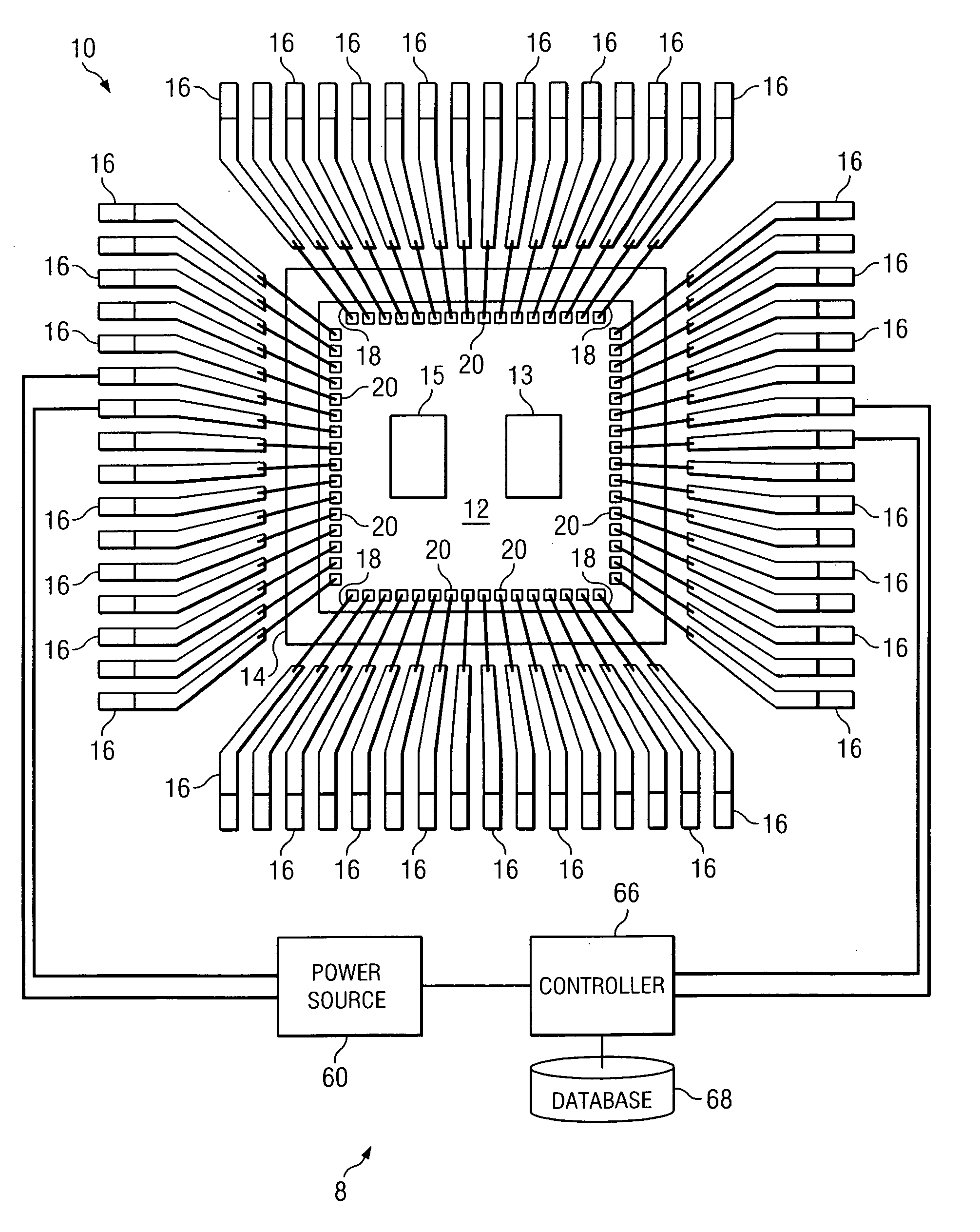
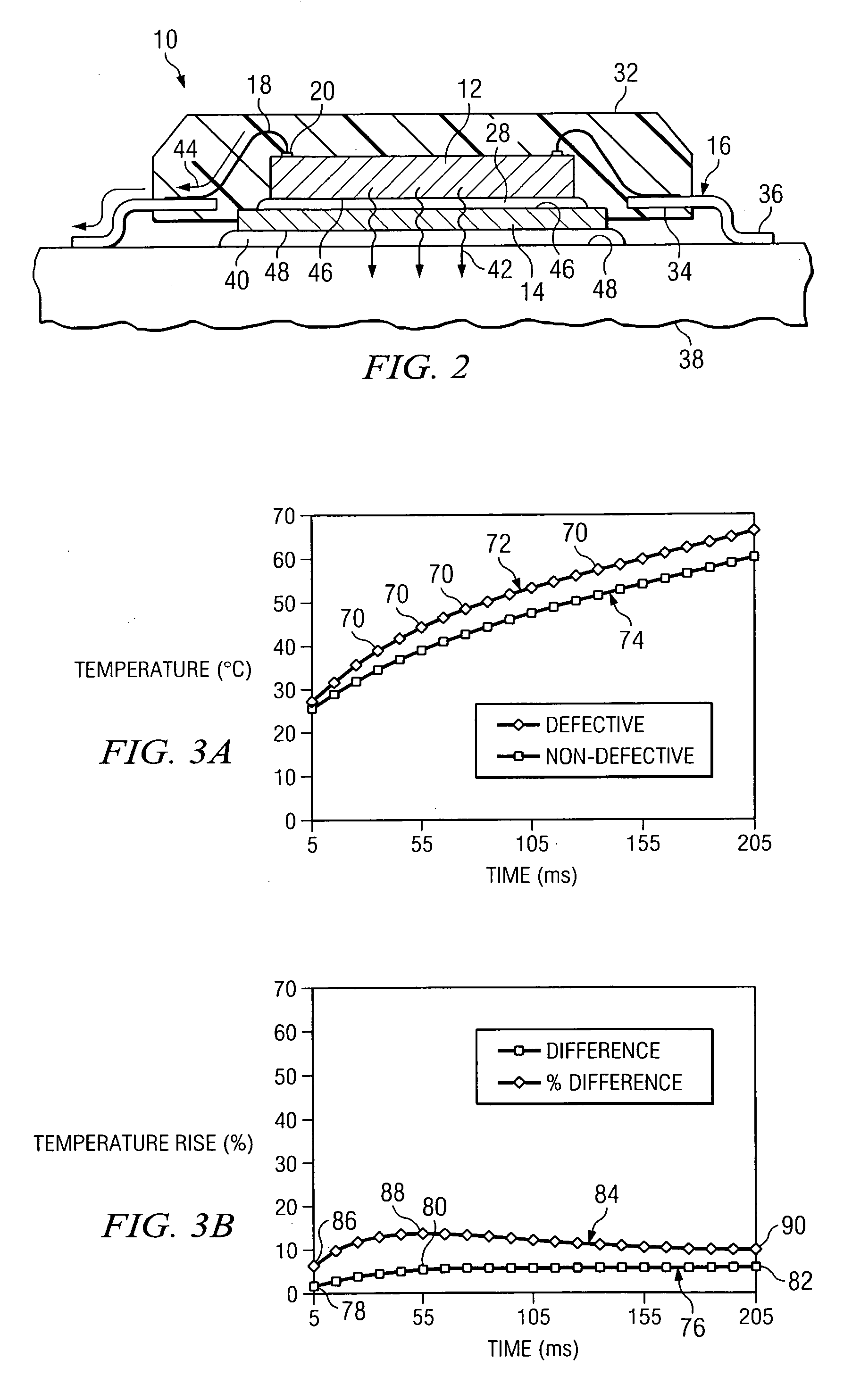
[0004] From the foregoing it may be appreciated by those skilled in the art that a need has arisen for a system and method for the detection of defects in an integrated circuit using thermal sensing. In accordance with the present invention, a system and method for detecting a defect in an integrated circuit using an optimized electrical pulse is provided that substantially eliminates or greatly reduces disadvantages and problems associated with conventional thermal measuring techniques.
[0005] According to one embodiment of the present invention, a method for detecting a defect in an integrated circuit using an optimized power pulse includes applying a first pulse of power to a first integrated circuit for an optimized pulse duration. The optimized pulse duration is determined as a function of a difference in temperature between a second, defective integrated circuit and a third, non-defective integrated circuit. The temperature of the first integrated circuit is measured after the...
PUM
 Abstract
Description
Claims
Application Information