Wafer support pin assembly

Inactive Publication Date: 2006-07-20
ASM AMERICA INC
View PDF17 Cites 342 Cited by
  • Summary
  • Abstract
  • Description
  • Claims
  • Application Information

AI Technical Summary

Benefits of technology

[0012] According to another aspect of the invention, a method is provided for assembling a semiconductor substrate support having a plurality of support structures. A susceptor having a plurality of bores extending therethrough from a top surface to a bottom surface is provided. An upper pin is passed through each of the plurality of bores, and each of the upper pins is engaged to a lower pin below the upper pin by rotating one of the upper pin and the lower pin by less than about 360 degrees.
[0013] According to yet another aspect of the invention, a process tool for processing semiconductor substrate is prov

Problems solved by technology

Certain areas of the backside of the substrate may be subject to particle contamination during and/or after one or more processing steps.
Such contamination may lead to or cause defects in the substrate.
Particles can also contaminate the processing environment within the reaction chamber, which can, in turn, contaminate a substrate being processed in the chamber.
The materials used in support pin assembly can cause also galling of the pin and guide, which also increases particles.
Such a threaded design typically requires vacuum vent holes to releasing undesirable trapped gas in the threaded connection between the pin head and the body of the pin due to a rise in process pressure.
These vent holes,

Method used


Image

  • Wafer support pin assembly
  • Wafer support pin assembly
  • Wafer support pin assembly

Examples


Embodiment Construction

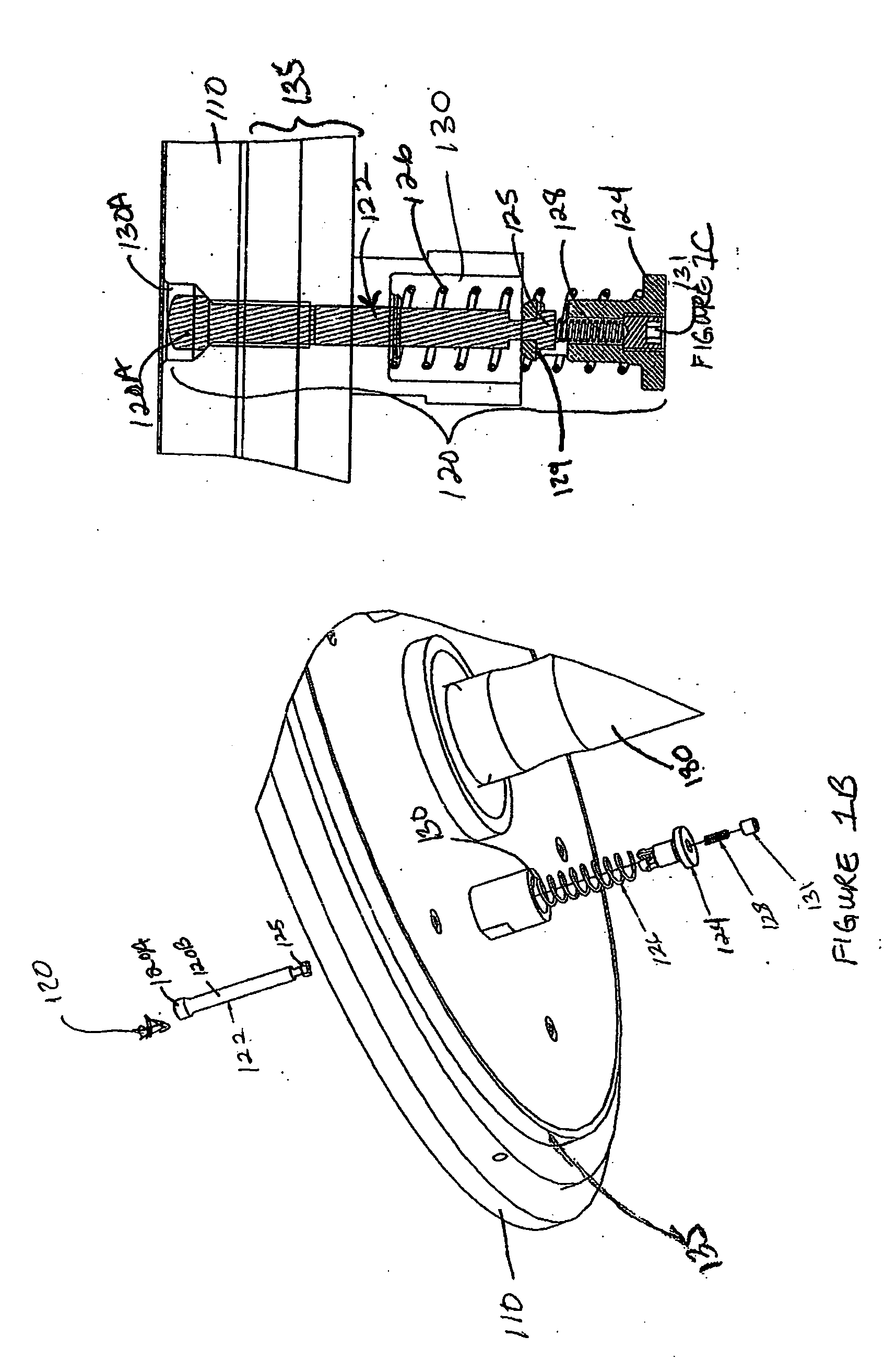
[0027] The following detailed description of the preferred embodiments and methods presents a description of certain specific embodiments to assist in understanding the claims. However, one may practice the present invention in a multitude of different embodiments and methods as defined and covered by the claims. For example, while the quick-release connection mechanism of the preferred embodiment is a bayonet mechanism, the skilled artisan will appreciate that other quick-release mechanisms can be hand-operated, without threaded screws or bolts.

[0028] Referring more specifically to the drawings for illustrative purposes, the present invention is embodied in the devices generally shown in the Figures. It will be appreciated that the apparatuses may vary as to configuration and as to details of the parts, and that the methods may vary as to the specific steps and sequence, without departing from the basic concepts as disclosed herein.

[0029] In an ALD process, gas delivery is used t...


PUM

PropertyMeasurementUnit
Angleaaaaaaaaaa
Angleaaaaaaaaaa
Heataaaaaaaaaa

Abstract

A semiconductor wafer support pin assembly. A susceptor has at least three support pins configured to raise a wafer above the top surface of the susceptor. Each support pin includes and upper pin and a lower pin, which lock together by means of a quick-release mechanism in the form of a bayonet mount. The upper pin is made of a non-metallic material, such as polybenzimidazole. The susceptor is driven up and down by a lifting mechanism, driven by an electric motor or pneumatic cylinder. The susceptor moves up and down, relative to the support pins.

Description

REFERENCE TO RELATED APPLICATIONS [0001] This application claims priority to U.S. Provisional Application No. 60 / 645,581, filed Jan. 18, 2005, and U.S. Provisional Application No. 60 / 656,832, filed Feb. 24, 2005.BACKGROUND OF THE INVENTION [0002] 1. Field of the Invention [0003] The field of the invention relates generally to semiconductor fabrication, and more particularly to a semiconductor substrate holder for processing semiconductor substrates. [0004] 2. Description of the Related Art [0005] Semiconductor processing steps typically employ various processing tools. Such processing tools include deposition devices, photolithography devices, polishing devices, etc. Most, if not all, of these devices use what is known as a substrate holding mechanism to hold a semiconductor substrate for processing. Some substrate holders or supports have a plurality (preferably at least three) of support pins that extend axially upward from a top surface of the substrate holder. The support pins c...

Claims


Application Information

Patent Timeline
IPC IPC(8): H01L21/44C23C16/00
CPCC23C16/4408C23C16/45525C23C16/45544C23C16/45563H01L21/68742C23C16/4586C30B35/00H01L21/67236H01L21/68714C23C16/45582H01L21/683C23C16/455C23C16/45517C23C16/45561C23C16/45587C23C16/45591C23C16/458C23C16/4582C23C16/4583H01L21/68785
Inventor FONDURULIA, KYLEWHITE, CARL
Owner ASM AMERICA INC
Why Eureka
Try Eureka