Semiconductor device

a technology of semiconductor chips and external terminals, applied in semiconductor devices, semiconductor/solid-state device details, electrical apparatus, etc., can solve the problems of inability to increase the number of terminals, the reduction of pitch is subject to fabrication technology limitations, and the inability to use this semiconductor chip, etc., to achieve the effect of increasing the maximum number of external terminals and increasing the cos

Inactive Publication Date: 2006-07-20
LAPIS SEMICON CO LTD
View PDF8 Cites 10 Cited by
  • Summary
  • Abstract
  • Description
  • Claims
  • Application Information

AI Technical Summary

Benefits of technology

[0011] A object of the present invention is to provide a technique for increasing the maximum number of external terminals being provided on the mount face of a semiconductor device that adopts a WCSP structure, without incurring a cost increase.
[0013] The semiconductor device according to the first standpoint of the present invention comprises a wiring region for providing second redistribution wiring and second external terminals. Therefore, the quantity of external terminals can be increased without reducing the rate of integration of the integrated circuit. Moreover, because the rate of integration of the integrated circuit is not reduced, the integrated circuit design can be shared by a chip mounted in a WCSP and a chip mounted in other type of package, and therefore the sharing of part of the fabrication process is then straightforward.
[0015] The semiconductor device according to the second standpoint of the present invention comprises a second region for providing second redistribution wiring structures and second external terminals. Therefore, the quantity of external terminals can be increased without reducing the rate of integration of the integrated circuit. Moreover, because the rate of integration of the integrated circuit is not reduced, the integrated circuit design can be shared by a chip mounted in a WCSP and a chip mounted in other type of package, and therefore the sharing of part of the fabrication process is then straightforward.

Problems solved by technology

In cases where the pitch is designated beforehand, it is not possible to increase the number of terminals by reducing the pitch.
In addition, the reduction in pitch is subject to fabrication technology limitations.
In a case where the degree of integration of the integrated circuit formed in the semiconductor chip is reduced, it is undesirable to use this semiconductor chip for fabricating a semiconductor device with a package structure other than a WCSP structure (a wire bonding structure, for example).
This is because, when wire bonding structure packaging or other non-WCSP packaging is performed on a semiconductor chip with a small degree of integration, the size of the semiconductor device is then abnormally large.
For this reason the design and fabrication process cannot be shared, and so the fabrication costs are extremely high.

Method used


Image

  • Semiconductor device
  • Semiconductor device
  • Semiconductor device

Examples


first embodiment

[0049] The first embodiment of the present invention will be described below.

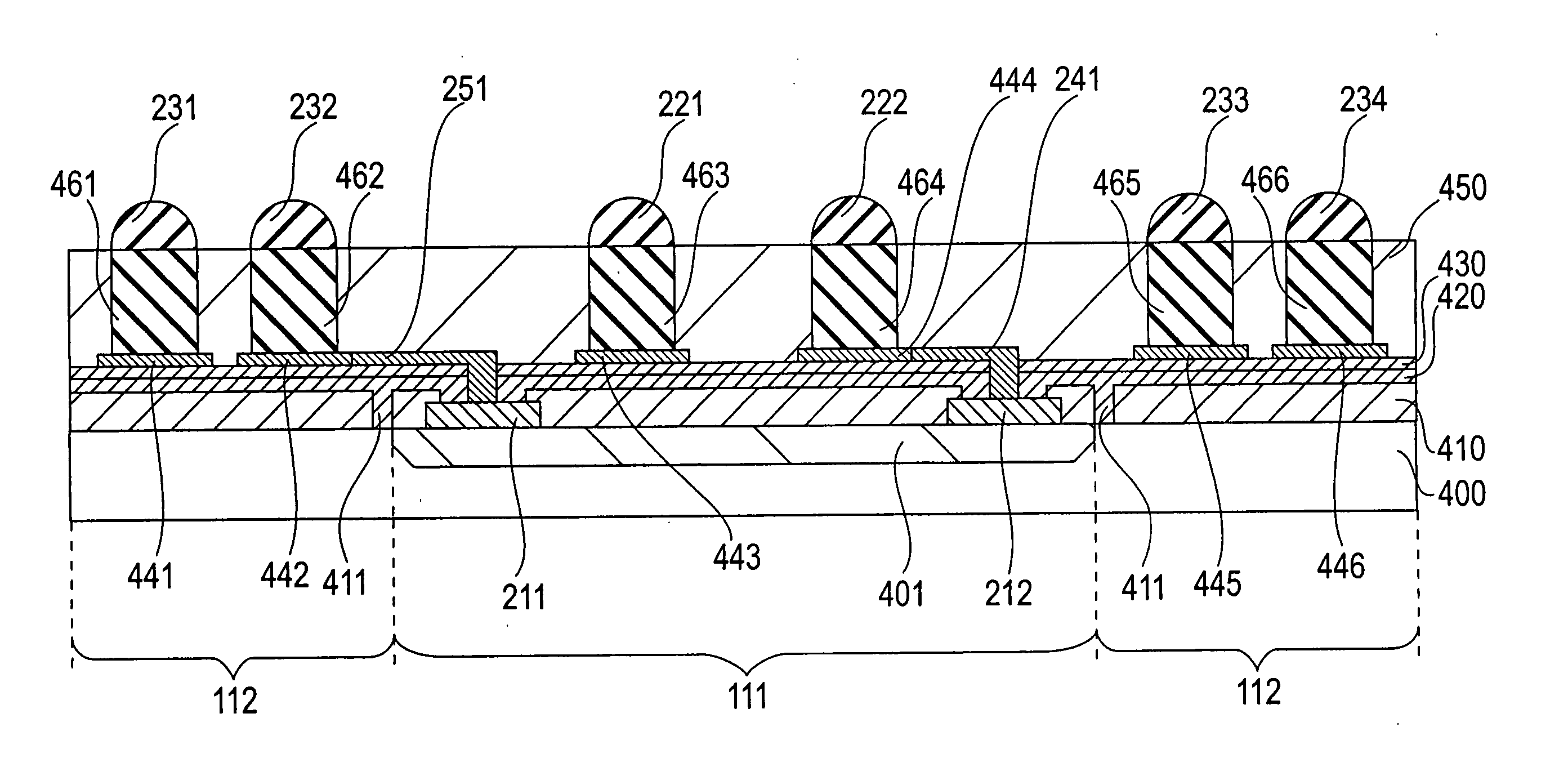
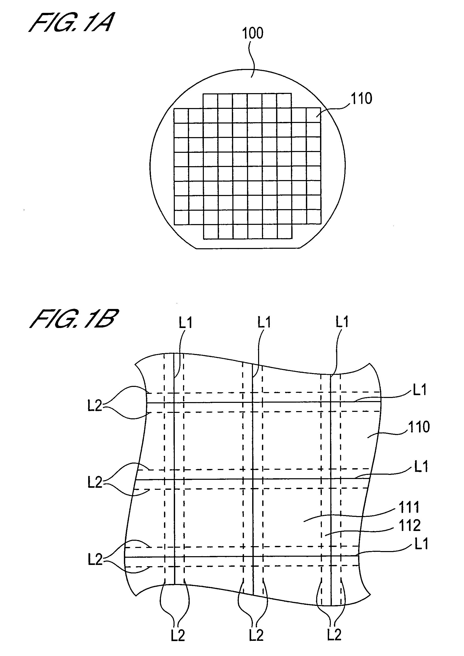
[0050]FIG. 1A is a planar view conceptually showing the structure of a semiconductor wafer according to this embodiment. As shown in FIG. 1A, a wafer 100 comprises a multiplicity of chip regions 110.

[0051]FIG. 1B is a partial enlarged view of FIG. 1A. In FIG. 1B, the solid lines L1 conceptually show the chip region boundaries. That is, the regions delimited by the lines L1 are the chip regions 110. Each of the chip regions 110 comprises a circuit region 111 and a wiring region 112. In FIG. 1B, the dotted lines L2 conceptually show the boundary between the circuit region 111 and the wiring region 112.

[0052] As will be described below, in the fabrication process for a semiconductor device that has a WCSP structure, the semiconductor wafer 100 is diced along the lines L1. On the other hand, in a fabrication process of a semiconductor device for which a package structure other than a WCSP structure is adopte...

second embodiment

[0100] The second embodiment of the present invention will be described next.

[0101] According to the first embodiment described above, a capacitor and an inductor are formed in the redistribution wiring layer (the layer sandwiched between the insulation layers 620 and 630 in FIG. 6). In contrast, the capacitor and inductor are formed below the redistribution wiring layer in the present embodiment.

[0102] The overall constitution of the semiconductor wafer according to this embodiment is the same as that of the semiconductor wafer of the first embodiment (FIGS. 1A and 1B) FIG. 13 is a planar view showing the structure below the redistribution wiring layer, of the present embodiment.

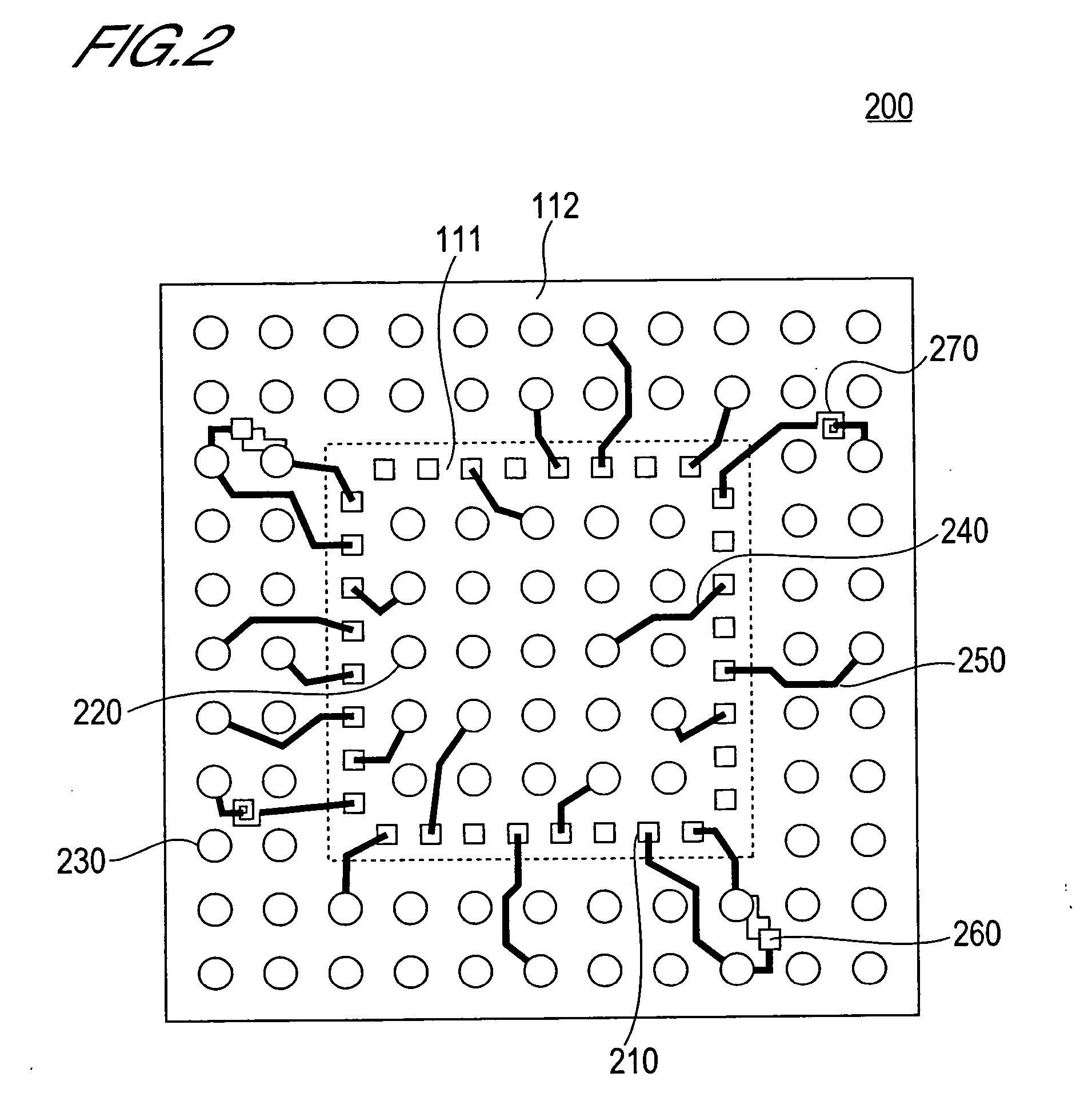
[0103] As shown in FIG. 13, the semiconductor chip 1300 of this embodiment comprises the circuit region 111 and the wiring region 112.

[0104] A plurality of electrode pads 210 is provided in the circuit region 111 as per the first embodiment (See FIG. 2).

[0105] Two capacitors 1311, 1312 and two inductor...

third embodiment

[0124] Next, the third embodiment of the present invention will be described.

[0125] The semiconductor device according to this embodiment differs from those of the first and second embodiments above in that the capacitor and inductor are formed in the wiring region 112 in the form of an array.

[0126]FIG. 19 is a planar view conceptually showing the semiconductor chip array formation face according to this embodiment. As shown in FIG. 19, a plurality of capacitors 1910 and a plurality of inductors 1920 are arranged alternately in the wiring region 112, for example. The passive element array is constituted by these capacitors 1910 and inductors 1920. The quantities of the capacitors 1910 and inductors 1920 and the dispositional order thereof, and so forth, can be optionally determined by the designer.

[0127] The capacitors 1910 and inductors 1920 are formed in a layer beneath the redistribution wiring layer as per the second embodiment (See FIGS. 15 and 16).

[0128] The size and chara...


PUM


Abstract

When an integrated circuit is formed in a semiconductor wafer, the integrated circuit is formed only in the central part of each chip region. In a case where packaging other than a chip size package is made, only the central part in which the integrated circuit is formed is cut from the wafer. In a case where a chip size package is made, the chip region is cut from the wafer after forming the redistribution wiring and external terminals and so forth over the whole of the chip region. As a result, the design of the integrated circuit and part of the fabrication process thereof can be shared by a chip which is mounted in a chip size package and a chip which is mounted in another type of package.

Description

BACKGROUND OF THE INVENTION [0001] 1. Field of the Invention [0002] The present invention relates to a semiconductor device. [0003] 2. Description of Related Art [0004] CSPs (Chip Size Packages) are known as semiconductor chip package structures. The adoption of a CSP makes it possible to make the size of the package substantially the same as the chip cut from the semiconductor wafer. [0005] WCSPs, which constitute one type of CSP, are known. Japanese Patent No. 3313547, for example, is known as a publication that discloses a WCSP. [0006] A WCSP structure comprises a redistribution wiring layer which is provided on the surface on which the integrated circuit is formed. External terminals, that is, input / output pins, are provided on the redistribution wiring layer. The redistribution wiring layer comprises wiring for connecting external terminals to the pads of the integrated circuit. In the above-mentioned publication, solder balls are employed as the external terminals. The surface...

Claims


Application Information

Patent Timeline
Patent Type & Authority Applications(United States)
IPC IPC(8): H01L23/52H01L23/12H01L23/31H01L23/522
CPCH01L23/3114H01L23/5222H01L23/5227H01L24/25H01L24/82H01L2224/18H01L2924/01002H01L2924/01004H01L2924/01013H01L2924/01029H01L2924/01056H01L2924/01078H01L2924/01079H01L2924/14H01L2924/19041H01L2924/30105H01L2924/30107H01L2924/01005H01L2924/01006H01L2924/01033H01L2924/014H01L2924/181
Inventor TERUI, MAKOTO
Owner LAPIS SEMICON CO LTD
Why Eureka
Try Eureka