Circuit board and manufacturing method therefor and semiconductor package and manufacturing method therefor

a manufacturing method and semiconductor technology, applied in the direction of functional valve types, sustainable manufacturing/processing, final product manufacturing, etc., can solve the problems of mounting reliability degradation connection is not achieved, etc., and achieve the effect of improving mounting reliability with respect to the mount substra

Inactive Publication Date: 2006-07-20
SONY CORP
View PDF3 Cites 17 Cited by
  • Summary
  • Abstract
  • Description
  • Claims
  • Application Information

AI Technical Summary

Benefits of technology

[0028] In the circuit board according to the embodiment of the present invention or a semiconductor package including a circuit board manufactured by the method for manufacturing the circuit board according to the embodiment of the present invention, the semiconductor package according to the embodiment of the preven

Problems solved by technology

With respect to the known semiconductor package, which has been described above, when the semiconductor package is mounted on a mount substrate by bonding the terminals of the mount substrate to solder balls, warpage occurs in the semiconductor package in a temperature atmosphere near the melting point of the solder balls, resulting in degradation in mounting reliability.
That is, when the semiconductor package is warped concavely, the solder balls in the peripheral regions of the

Method used


Image

  • Circuit board and manufacturing method therefor and semiconductor package and manufacturing method therefor
  • Circuit board and manufacturing method therefor and semiconductor package and manufacturing method therefor
  • Circuit board and manufacturing method therefor and semiconductor package and manufacturing method therefor

Examples


Embodiment Construction

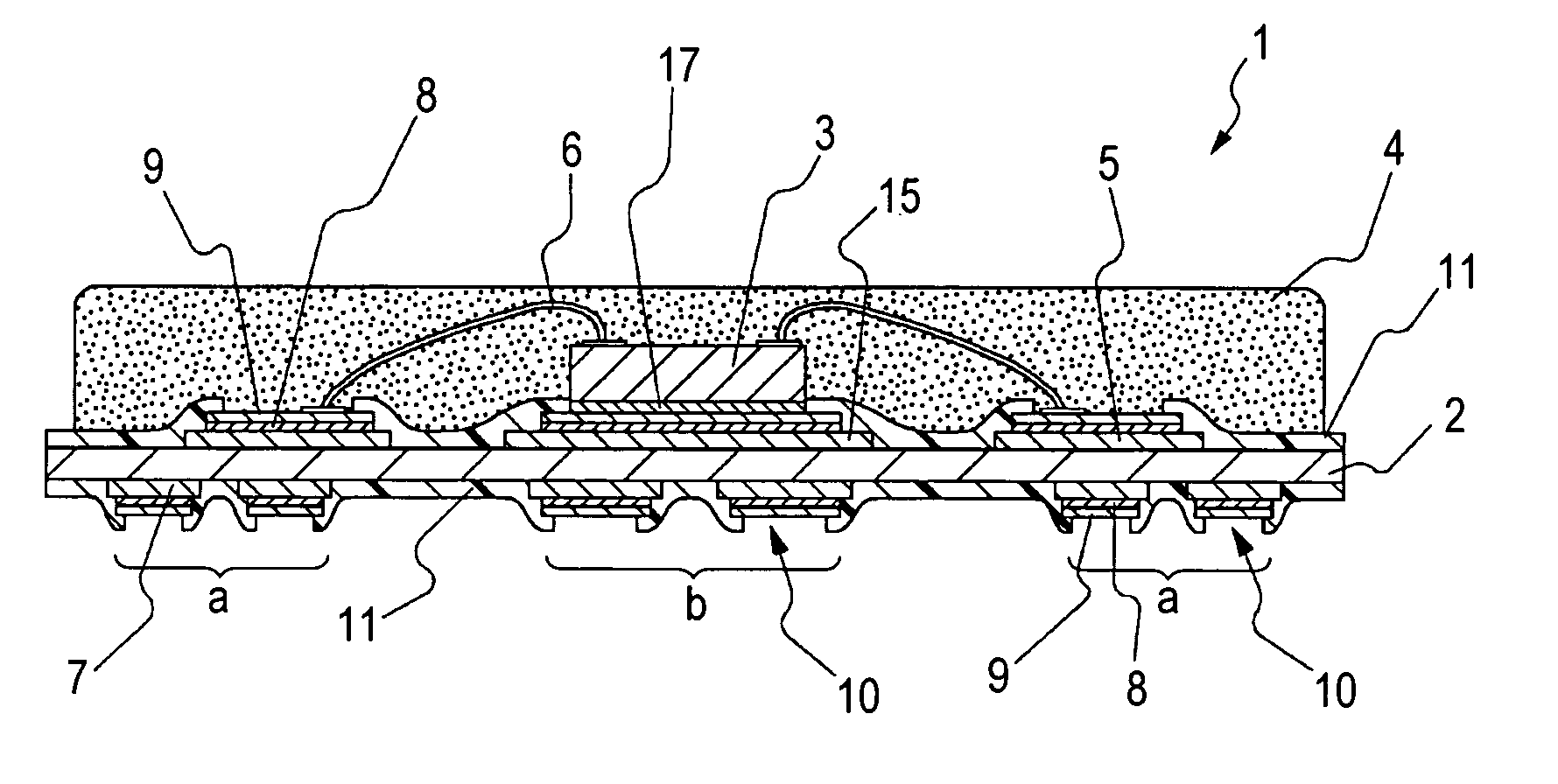
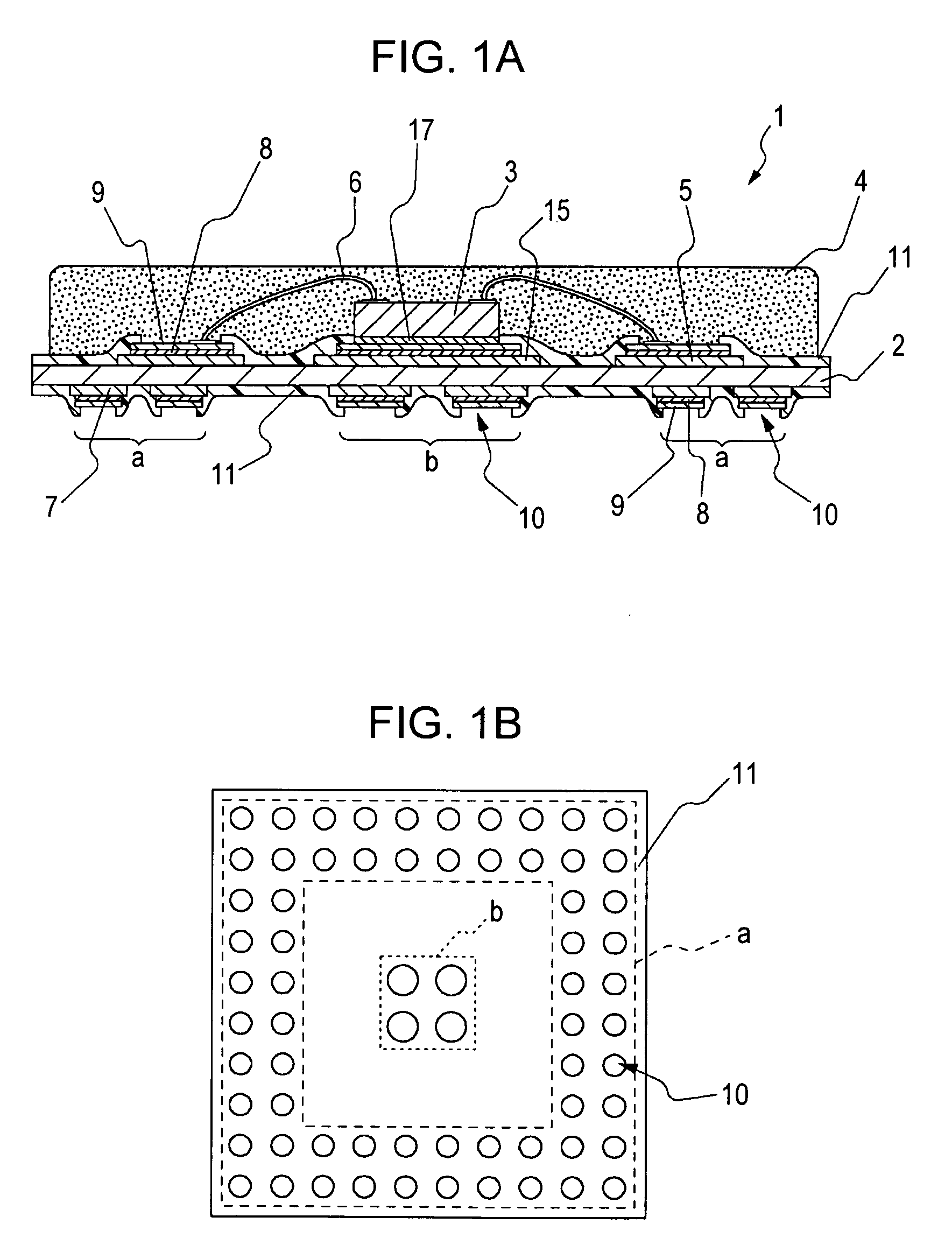
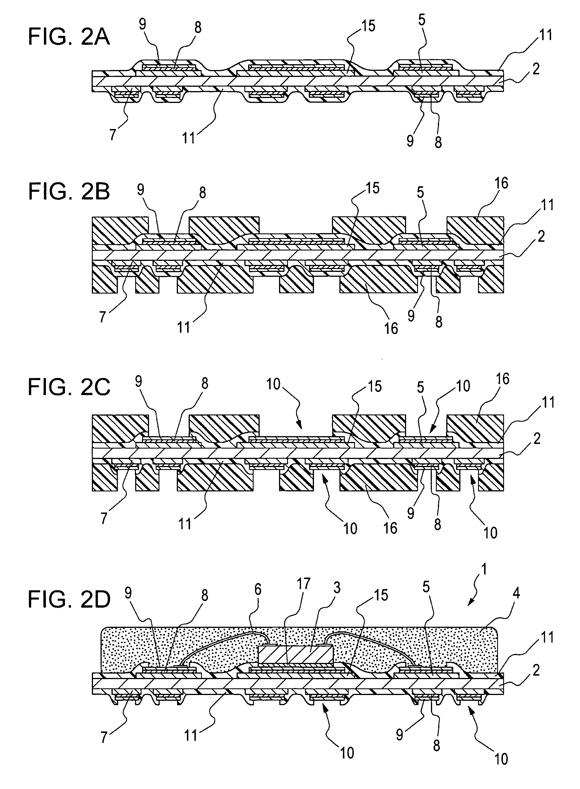
[0038] Embodiments of the present invention will be described with reference to the drawings. In the embodiments below, a semiconductor package in which concave warpage occurs when the semiconductor package is mounted on a mount substrate will be described as an example (refer to FIG. 8A).

[0039]FIGS. 1A and 1B are a schematic sectional view and a schematic bottom view, respectively, of a semiconductor package according to an embodiment of the present invention. A semiconductor package 1 includes an interposer substrate 2, a semiconductor chip 3 die-bonded to the upper surface of the interposer substrate 2, and a sealing resin 4 which seals the semiconductor chip 3, similar to the semiconductor package 101 described above.

[0040] Each chip electrode of the semiconductor chip 3 is wire-bonded via a thin gold wire 6 to an outgoing line of a chip mount surface wiring pattern 5 formed on a chip mount surface of the interposer substrate 2. The chip mount surface wiring pattern 5 is conne...


PUM


Abstract

A circuit board includes a circuit board body having a semiconductor device mounting area for mounting a semiconductor device, a wiring pattern to be electrically connected to a semiconductor device to be mounted on the semiconductor device mounting area, and an insulating layer for covering the wiring pattern, the insulating layer having openings formed therein at regions on which bumps for electrically connecting the wiring pattern to a mount substrate are disposed. The opening sizes of the openings are allowed to vary depending on the positions at which the openings are formed.

Description

CROSS REFERENCES TO RELATED APPLICATIONS [0001] The present invention contains subject matter related to Japanese Patent Application JP 2005-013244 filed in the Japanese Patent Office on Jan. 20, 2005, the entire contents of which are incorporated herein by reference. BACKGROUND OF THE INVENTION [0002] 1. Field of the Invention [0003] The present invention relates to a circuit board and a manufacturing method therefor and a semiconductor package and a manufacturing method therefor. More particularly, the invention relates to a circuit board in which good terminal flatness is achieved, thus improving the mounting yield, a method for manufacturing the circuit board, a semiconductor package including such a circuit board, and a method for manufacturing the semiconductor package. [0004] 2. Description of the Related Art [0005] With the reduction in size and weight, increase in operational speed, and increase in functionality of electronic equipment, miniaturization and integration of se...

Claims


Application Information

Patent Timeline
IPC IPC(8): H01L23/48H01L23/52H01L29/40
CPCH01L23/3128H01L23/49816H01L23/49822H01L2224/32225H01L2224/48091H01L2224/48227H01L2224/73265H01L2224/92247H01L2924/01005H01L2924/01033H01L2924/01078H01L2924/01079H01L2924/01082H01L2924/15311H01L2924/3511H05K3/3436H05K3/3452H05K2201/094H05K2203/0465H01L2924/00014H01L24/32H01L24/48H01L2924/01006H01L2224/45144H01L2924/00H01L2924/00012H01L24/45H01L24/73H01L2924/181Y02P70/50H01L2224/45015H01L2924/207B05B1/306B05B12/002B05B13/0278F16J15/02F16K15/044
Inventor HOKARI, SUMIO
Owner SONY CORP
Why Eureka
Try Eureka