Method of predicting high-k semiconductor device lifetime

a technology of semiconductor devices and lifetime prediction, applied in the direction of measurement devices, semiconductor operation lifetime testing, instruments, etc., can solve the problems of bias temperature instability, high-k gate dielectric layer device performance problems, and higher speed adversely affecting device performan

Inactive Publication Date: 2006-07-20
TAIWAN SEMICON MFG CO LTD
View PDF21 Cites 24 Cited by
  • Summary
  • Abstract
  • Description
  • Claims
  • Application Information

AI Technical Summary

Benefits of technology

[0008] These and other problems are generally solved or circumvented, and technical advantages are generally achieved ...

Problems solved by technology

There are, however, device performance problems associated with high-k gate dielectric layers.
The increased electric field needed for higher speed adversely affects device performance through hot carrier (HC) injection and trap generation.
High trap density also leads to leakage through Frenkel-Poole tunneling, and it causes bias temperature instability.
Given the ever-increasing demand for improved device performance, hot carrier damage is one of the mos...

Method used


Image

  • Method of predicting high-k semiconductor device lifetime
  • Method of predicting high-k semiconductor device lifetime
  • Method of predicting high-k semiconductor device lifetime

Examples


Embodiment Construction

[0023] The operation and fabrication of the presently preferred embodiments are discussed in detail below. However, the embodiments and examples described herein are not the only applications or uses contemplated for the invention. The specific embodiments discussed are merely illustrative of specific ways to make and use the invention, and do not limit the scope of the invention or the appended claims.

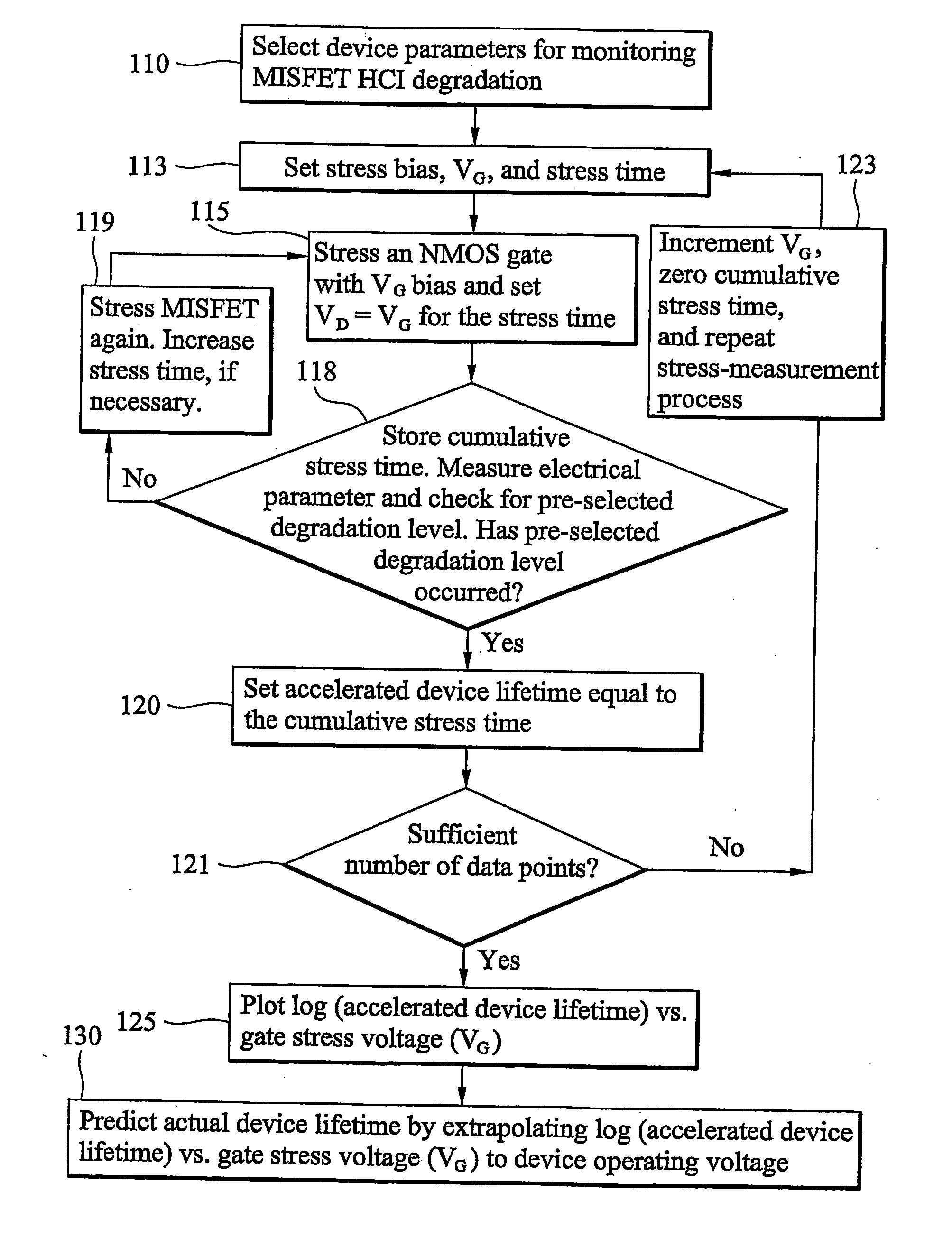
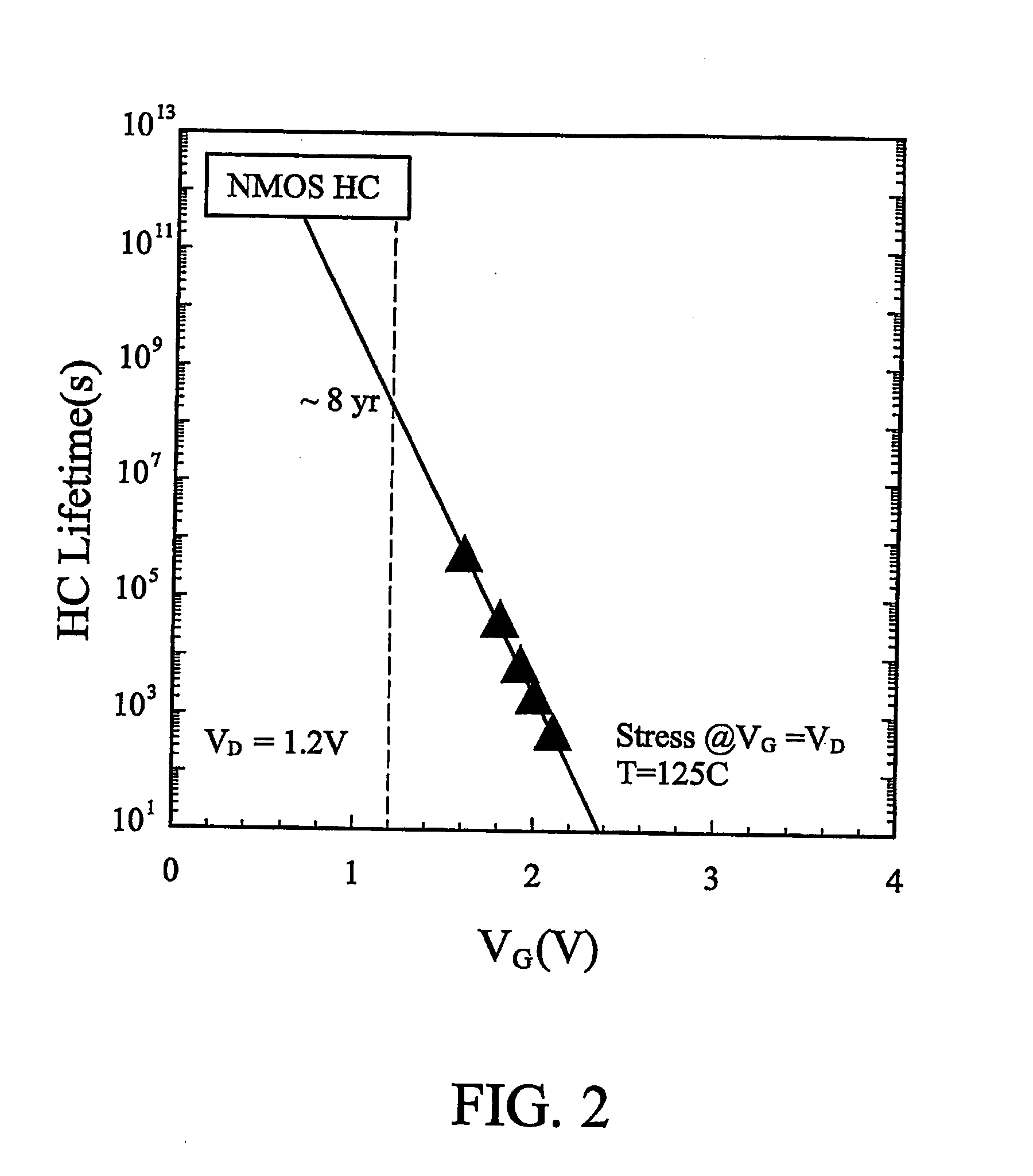
[0024] The present invention will now be described with respect to preferred embodiments in a specific context, namely predicting the lifetime of an integrated circuit using hot carrier injection (HCI) accelerated stress measurements of a NMOS. A stress voltage is applied at both the gate and the drain, the stress gate voltage being appropriate for inducing positive bias temperature instability (PBTI) degradation in a NMOS transistor. It is believed that embodiments of this invention are particularly advantageous when used in this process. It is further believed that embodiments desc...


PUM


Abstract

A preferred embodiment of the invention provides a method for testing a MISFET to determine the effect of hot carrier injection (HCI) on integrated circuit lifetime. The method comprises applying a positive stress voltage to a gate having a high-k dielectric, while simultaneously holding a drain voltage equal to the stress voltage. Using a stress voltage that is greater than a normal operating voltage accelerates the degradation and failure of the integrated circuit. Embodiments include monitoring electrical parameters such as threshold voltage, transconductance, linear drain current, or saturation drain current. A pre-selected shift in a monitored electrical parameter indicates device failure. Embodiments include analyzing the data by plotting the logarithm of an accelerated device lifetime versus the gate stress voltage. The device lifetime under operating conditions is predicted by extrapolating the plot for a given device operating voltage.

Description

[0001] This application claims the benefit of U.S. Provisional Application No. 60 / 642,574, filed on Jan. 10, 2005, entitled Method of Predicting High-K Semiconductor Device Lifetime, which application is hereby incorporated herein by reference.TECHNICAL FIELD [0002] This invention relates generally to the fabrication of semiconductor devices, and more particularly to the prediction of device lifetime degradation caused by hot carrier effects in high dielectric constant (high-k) gate dielectrics. BACKGROUND [0003] As metal insulator semiconductor field effect transistor (MISFET) feature sizes decrease, the gate oxide thickness of the devices also decreases. This decrease is driven in part by the demands of overall device scaling. As gate conductor widths decrease, for example, other device dimensions decrease to maintain the proper device scale, and thus device operation. Another factor driving reduction of the gate oxide thickness is the increased transistor drain current realized f...

Claims


Application Information

Patent Timeline
IPC IPC(8): G01R31/26
CPCG01R31/2621G01R31/2642H01L21/18H01L21/02
Inventor TSAI, CHING-WEIWANG, CHIH-HAOCHI, MIN-HWA
Owner TAIWAN SEMICON MFG CO LTD
Why Eureka
Try Eureka