Light emitting device

Inactive Publication Date: 2006-07-20
PANASONIC CORP
View PDF10 Cites 7 Cited by
  • Summary
  • Abstract
  • Description
  • Claims
  • Application Information

AI Technical Summary

Benefits of technology

[0020] Due to a sudden change of an electric potential after stopping the voltage application, the residual charge brings to a generation of a counter electromotive force in the light emitting element. Accordingly, at the time of discharging the residual charge, if the light emitting element has a failed structural part with a low resistance, the reverse current flows rapidly with concentrated on the failed structural part. In result, there is no necessity for the light emitting element to use a power supply voltage as a reverse bias in order to eliminate the disadvantageous effect caused from the failed structural part. Since only the residual charge is used, there is no danger that the reverse current becomes excessive enough to destroy the light emitting element.
[0021] A circuit, in order to feed the reverse current to the light emitting element after application of the DC forward voltage, may only connect respective electrodes of the light emitting element applied with the DC forward voltage with the earth, for example. If the light emitting element is an organic electro luminescence diode, both electrodes of the diode are connected to the earth. A use of such circuit can reduce the circuit cost, simplify the control process, and downsize the apparatus along with extending the life of the light emitting element.
[0022] When the light emitting element is used as a light source for the printer and the display unit, the steps of applying of the DC forward voltage and stopping the app

Problems solved by technology

Accordingly, if a current with a given value is fed hereto, it is hard to obtain the desired luminous intensity.
Moreover, owing to the concentration of the electric charge, the black spot slowly destroys the organic EL layer surrounding itself, and this cau

Method used


Image

  • Light emitting device
  • Light emitting device
  • Light emitting device

Examples


Example

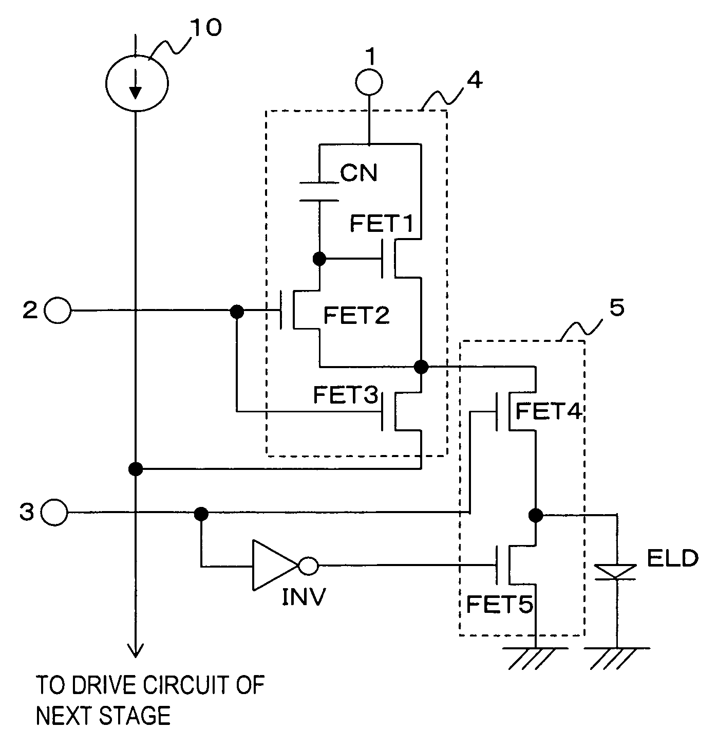
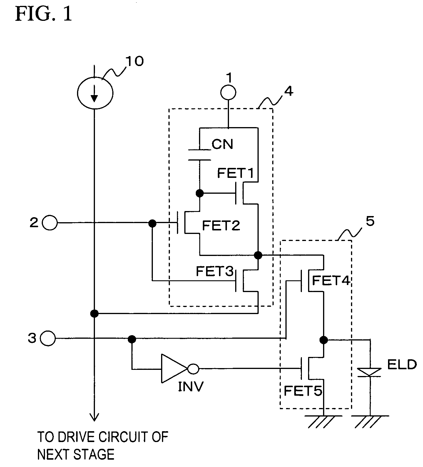
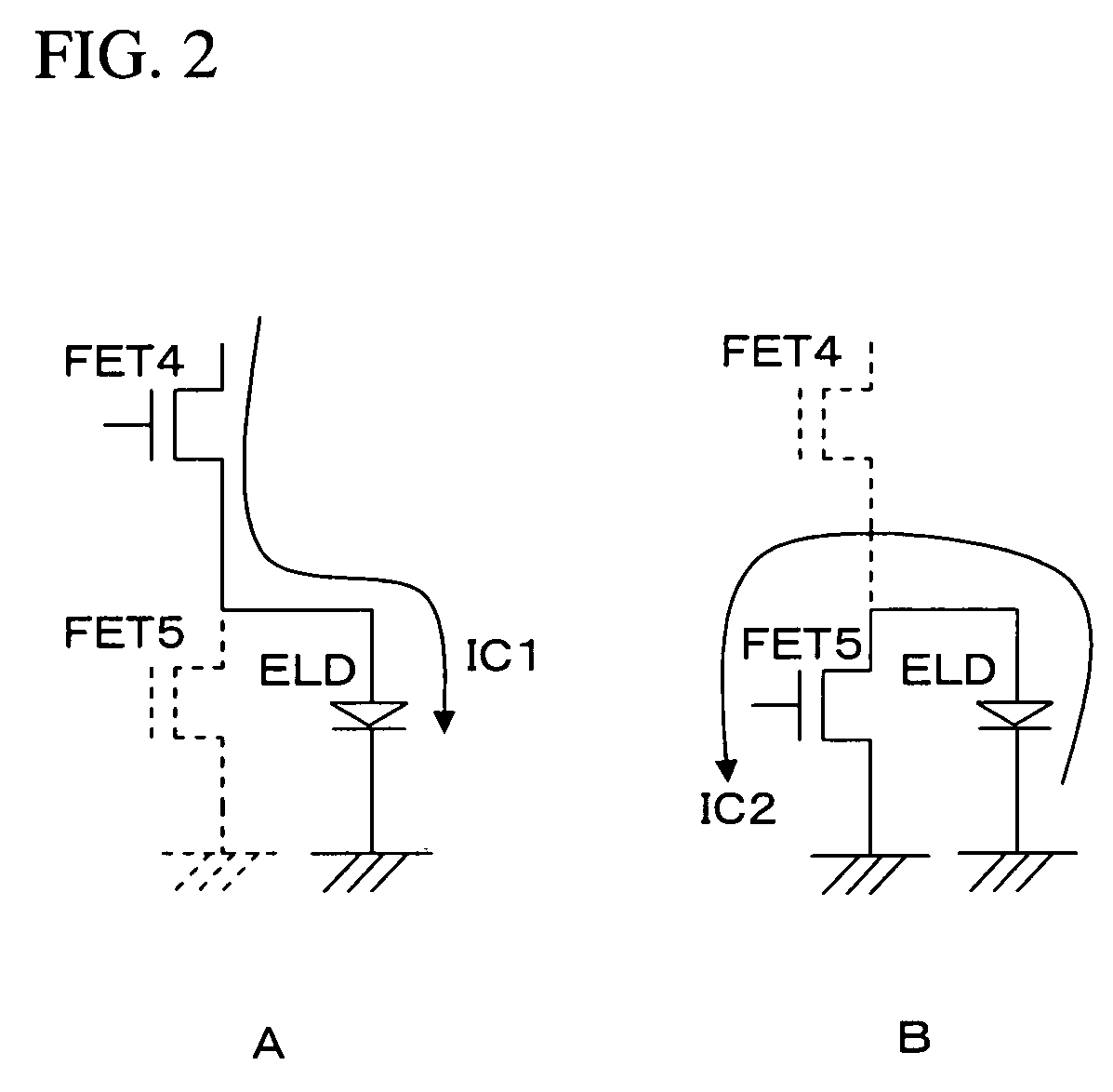
[0039] In this embodiment, a light emitting device of the invention is materialized as a print-head included in a printing system. The print-head has a plurality of organic EL elements ELD as a capacitive light emitting element, and by controlling the light and extinction of each organic EL element based on an input image, a latent image corresponding to the image can be formed on a photo conductor. Like the conventional art shown in FIG. 9, the print-head has plural sets of an organic EL eminent and the drive circuit 9, and one of those drive circuits is illustrated by FIG. 1.

[0040] A current for lighting the organic EL element ELD is fed from a current feeding circuit 4. And in this embodiment, a current copier circuit is used to the current feeding circuit 4. The current copier circuit includes switching elements FET1, FET2, and FET3, and a capacitor CN as a capacitive element for accumulating an electric charge, like the conventional art. The work is also the same as the conven...


PUM


Abstract

A light emitting device capable of feeding a reverse current to the defective structural part of a light emitting element, e.g. an organic EL element, without using the power supply voltage as reverse bias. The light emitting device comprises a capacitive light emitting element, e.g. an organic EL element, emitting light upon application of a DC forward voltage. A reverse current can be fed to the light emitting element through a low-resistance defective structural part, for example, only by connecting both electrodes of the organic EL element with the earth after sopping application of the DC forward voltage using a push-pull circuit (5), thereby discharging residual charges of the light emitting element.

Description

TECHNICAL FIELD [0001] The invention relates to a light emitting device provided with a capacitive light emitting element, such as an organic light emitting element utilizing the organic Electroluminescence, and available to a light source or a display unit for forming an electrostatic latent image on a photosensitive conductor of an image forming apparatus, or the like. BACKGROUND ART [0002] As exemplified by Japanese laid-open publication No. 11-198433, an organic light emitting device is applied to a print-head for forming an image on a photo conductor of an image forming apparatus such as a printer, as well as to a display. The print-head 11, as shown in FIG. 9, is designed so that plural sets of an organic EL element drive circuit 9 and an organic EL element ELD are disposed in line abreast, and the number of them becomes several thousand and over. One of the plural organic EL element drive circuits 9 has a configuration as shown in FIG. 10, for example. [0003] Referring to FIG...

Claims


Application Information

Patent Timeline
IPC IPC(8): G09G3/30G09G3/32H01L27/32H05B44/00
CPCG09G3/325G09G2300/0842G09G2300/0861G09G2310/0256G09G2330/08G09G2330/10H01L27/3244H05B33/0896H05B45/60Y02B20/30H10K59/12
Inventor MASUMOTO, KEN-ICHINAKAMURA, TETSUROH
Owner PANASONIC CORP
Why Eureka
Try Eureka