Radio frequency switch

a radio frequency switch and frequency technology, applied in electronic switching, pulse technique, semiconductor/solid-state device details, etc., can solve the problems of low power handling efficiency, signal leakage through capacitance, and leakage current degrade isolation, so as to improve power handling and low cost

Inactive Publication Date: 2006-07-20
SUMITOMO ELECTRIC DEVICE INNOVATIONS
View PDF29 Cites 64 Cited by
  • Summary
  • Abstract
  • Description
  • Claims
  • Application Information

AI Technical Summary

Benefits of technology

[0012] It is a general object of the present invention to solve the above-mentioned problems and provide a radio frequency switch. More specifically, the voltage applied to the FETs connected in series in the off state is equally divided, and the handling power is improved easily and at a low cost.

Problems solved by technology

This results in a problem in that a handling power becomes smaller than a value calculated from the following logical formula 1.
However, the conventional technique disclosed in Document 1 and shown in FIG. 4 has a problem in which a signal is leaked through the capacitances C1 and C2.
This leakage current degrades isolation at the time of switching off.
Additionally, there is still another problem in that the FETs are required to have a high breakdown voltage, as compared to the circuit without the capacitances Ca and Cb.
Therefore, it is no longer possible to solve the above-mentioned problems with the conventional techniques disclosed in Documents 1 through 3, which have the problems in terms of the breakdown voltages.

Method used


Image

  • Radio frequency switch
  • Radio frequency switch
  • Radio frequency switch

Examples


first embodiment

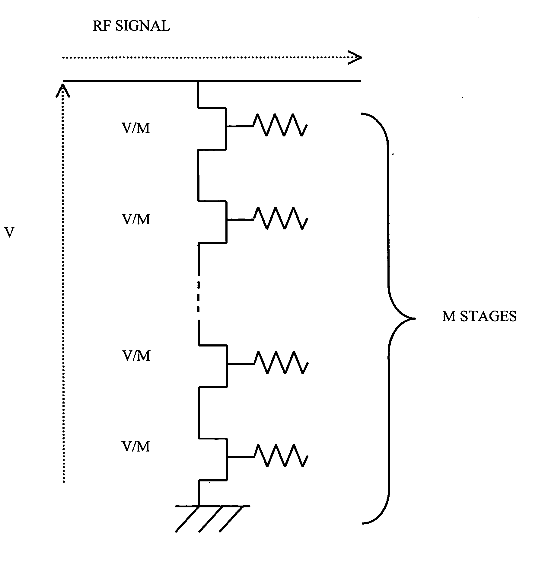
[0027]FIG. 7A is a plan view of an RF switch in accordance with a first embodiment of the present invention. The RF switch in FIG. 7A includes FETs connected in series at three stages. FIG. 7B shows a conventional RF switch having the FETs connected in series at three stages. As will be described below, the width of an electrode interconnection that is connected to a source or drain of the FET at an intermediate (second) stage is narrower than another electrode interconnection that is connected to the source or drain of the FET at an initial (first) stage and an RF line or that is connected to the source or drain of the FET at a final (third) stage and a ground line. The electrode interconnection that is connected to the source of the FET is referred to as a source electrode. The electrode interconnection that is connected to the drain of the FET is referred to as a drain electrode.

[0028] Three FETs 101, 102, and 103 are arranged in three separate FET-forming regions 161, 162, and ...

second embodiment

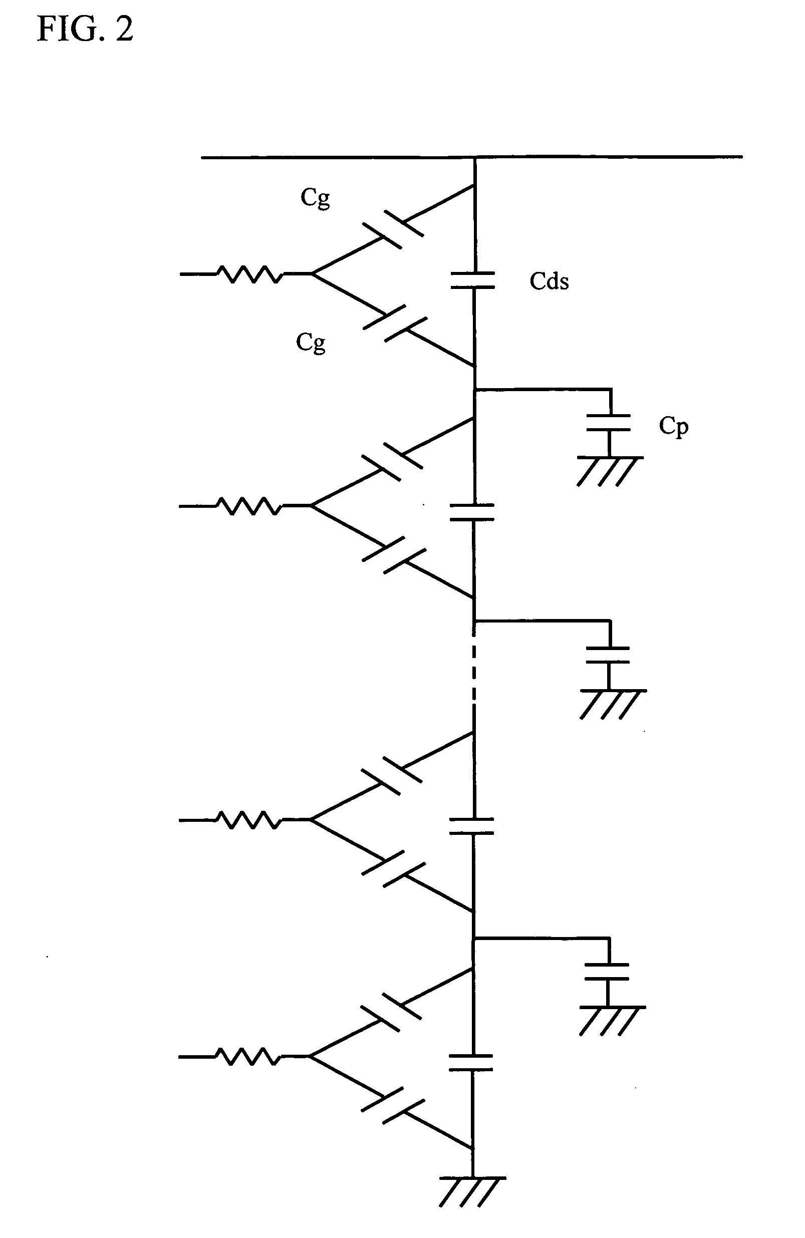
[0037]FIG. 9 is a plan view of an RF switch in accordance with a second embodiment of the present invention. Hereinafter, in the second embodiment, the same components and configurations as those of the first embodiment have the same reference numerals. In accordance with the second embodiment of the present invention, the total gate width of the FETs that are arranged in the FET-forming regions 162 at the intermediate (second in the present embodiment) stage(s) is configured to be smaller than the total gate width of the FETs at the initial and final stages. More specifically, each of the FET-forming regions 161 and 163 includes seven FETs. In contrast, the FET-forming region 162 includes six FETs. It is thus possible to reduce the total area of the S / D electrode interconnections 301 and 302, as compared to that in the circuit shown FIG. 7A, and to thereby further reduce the parasitic capacitance Cp to ground. This makes it possible to realize the RF switch having a higher handling...

third embodiment

[0038]FIG. 10 is a plain view of an RF switch in accordance with a third embodiment of the present invention. Hereinafter, in the second embodiment, the same components and configurations as those of the first embodiment have the same reference numerals. The third embodiment has an arrangement in which the FETs arranged in the FET-forming regions 162 at the second (intermediate) stage have a size smaller than that of the FETs at the first and third stage. It is thus possible to further reduce the parasitic capacitance Cp to ground, by shortening the total length of the S / D electrode interconnections 301 and 302. This makes it possible to realize the RF switch having a higher handling power, by lowering the parasitic capacitance Cp to ground without costly additional capacitances and degrading the surge resistance. The third embodiment may be combined with the second embodiment of the present invention.


PUM


Abstract

A switch that selectively changes radio frequency signals includes at least three FETs, which are connected in series. The source electrodes or drain electrodes arranged at an intermediate stage have a width narrower than that of the source electrodes or the drain electrodes arranged at the initial and final stages. It is thus possible to lower the parasitic capacitance to ground at the intermediate stage and to thereby realize the switch having a high handling power.

Description

BACKGROUND OF THE INVENTION [0001] 1. Field of the Invention [0002] This invention generally relates to a radio frequency (RF) switch that is used for a radio frequency device such as a mobile telecommunications device, and more particularly, to the radio frequency switch on which multiple FETs are connected in series. [0003] 2. Description of the Related Art [0004] In recent years, an RF switch having multiple ports (SPNT: Single Pole N-Through: N denotes the number of ports) has been employed in a mobile telephone unit, which communicates over multiple carrier signals. The RF switch includes a field-effect transistor (FET) composed of compound semiconductors. The RF switch is required to have a low harmonic performance, more specifically −70 dBc or less, to a fundamental harmonic of a transmitting signal. In order to suppress a harmonic component at a low level, the FET is required to improve linearity in the on-state resistance and to have an excellent off-state power. [0005] In ...

Claims


Application Information

Patent Timeline
Patent Type & Authority Applications(United States)
IPC IPC(8): H04B1/28H01L21/822H01L27/04H01L27/095H03K17/10
CPCH01P1/15H03K17/102H04B1/44
Inventor MIYAZAWA, NAOYUKI
Owner SUMITOMO ELECTRIC DEVICE INNOVATIONS
Why Eureka
Try Eureka