Semiconductor device and method for manufacturing semiconductor device

a semiconductor and semiconductor technology, applied in semiconductor devices, semiconductor/solid-state device details, electrical apparatus, etc., can solve the problems of large material cost of printed circuit boards, cost increase, and difficulty in manufacturing packages with predetermined outer dimensions, and achieve the effect of widening the wires

Inactive Publication Date: 2006-07-27
SHARP KK
View PDF4 Cites 40 Cited by
  • Summary
  • Abstract
  • Description
  • Claims
  • Application Information

AI Technical Summary

Benefits of technology

[0015] The present invention has as an object to provide: (i) a semiconductor device which makes it possible to place external connection pads at greater intervals, and which makes it possible to widen wires and to place the wires at greater intervals; and (ii) a method for manufacturing the semiconductor device.

Problems solved by technology

The printed circuit board takes up a large part of the cost of material required for the manufacture of the CSP.
This requires an improvement in processing accuracy, which causes cost increase.
Therefore, as in the case of the conventional package, it is difficult to manufacture packages with predetermined outer dimensions.
However, when the number of pins increases, the bumps inevitably make contact with one another.

Method used


Image

  • Semiconductor device and method for manufacturing semiconductor device
  • Semiconductor device and method for manufacturing semiconductor device
  • Semiconductor device and method for manufacturing semiconductor device

Examples


first embodiment

[0043] A first embodiment of the present invention will be described below with reference to FIGS. 1(a) to 6. Note that the present invention is not limited to this.

[0044] (An Arrangement of a Semiconductor Device)

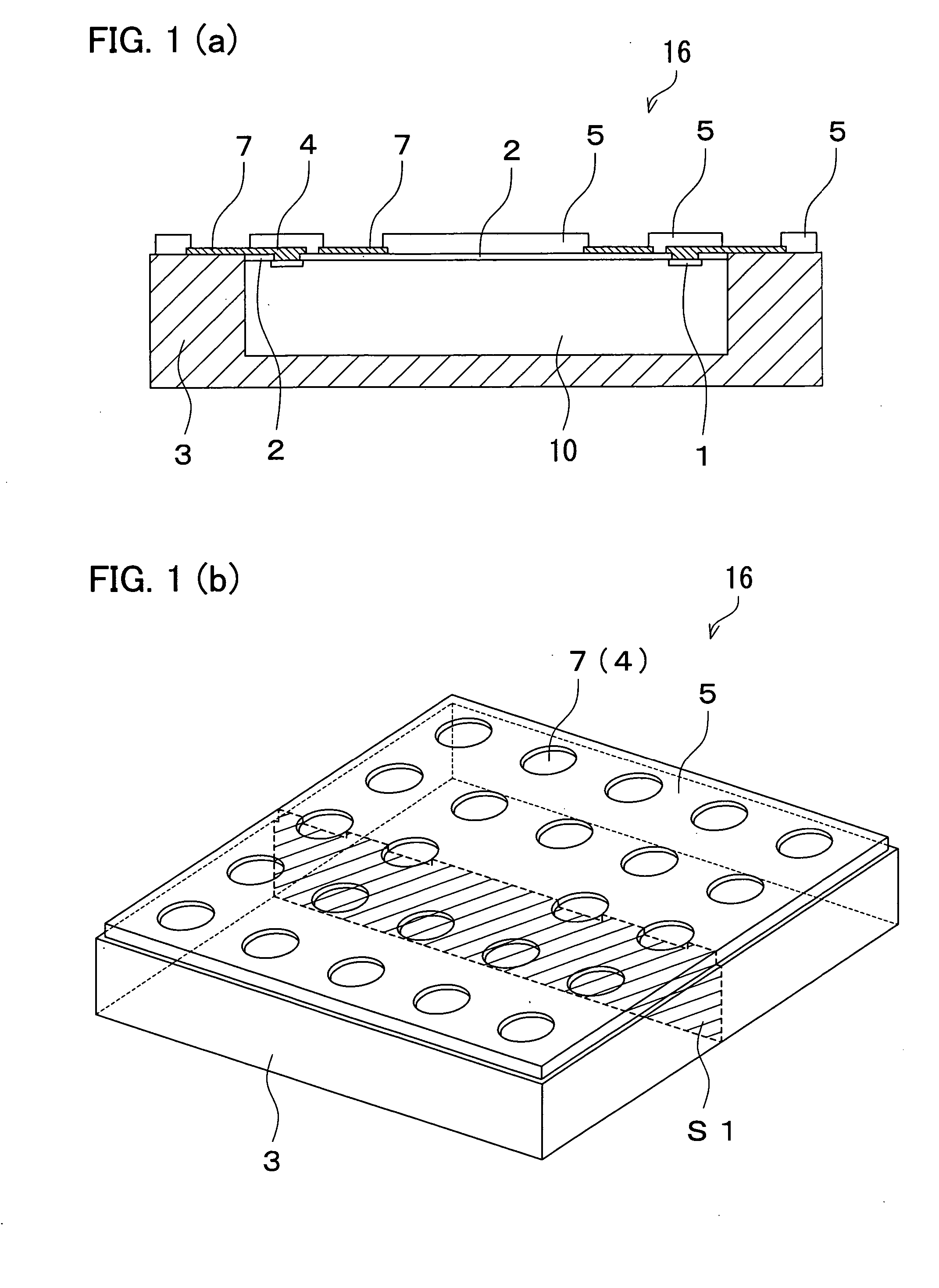
[0045] First, an arrangement of a semiconductor device of the present embodiment will be described. FIG. 1(b) is a perspective view of a semiconductor device 16 of the present embodiment. FIG. 1(a) is a cross-sectional view taken along surface S1 of FIG. 1(b).

[0046] As illustrated in FIG. 1(a), the semiconductor device 16 of the present embodiment includes a semiconductor chip 10, a sealing resin (insulating section) 3, metal wires (wires) 4, external connection pads 7, and a protective resin 5.

[0047] The semiconductor chip 10 has electrode pads 1. The semiconductor chip 10 is covered with an insulating film 2 so that an upper surface of each of the electrode pads 1 is exposed. That is, the insulating film 2 is not applied over the upper surface of the electrode pad 1 ...

second embodiment

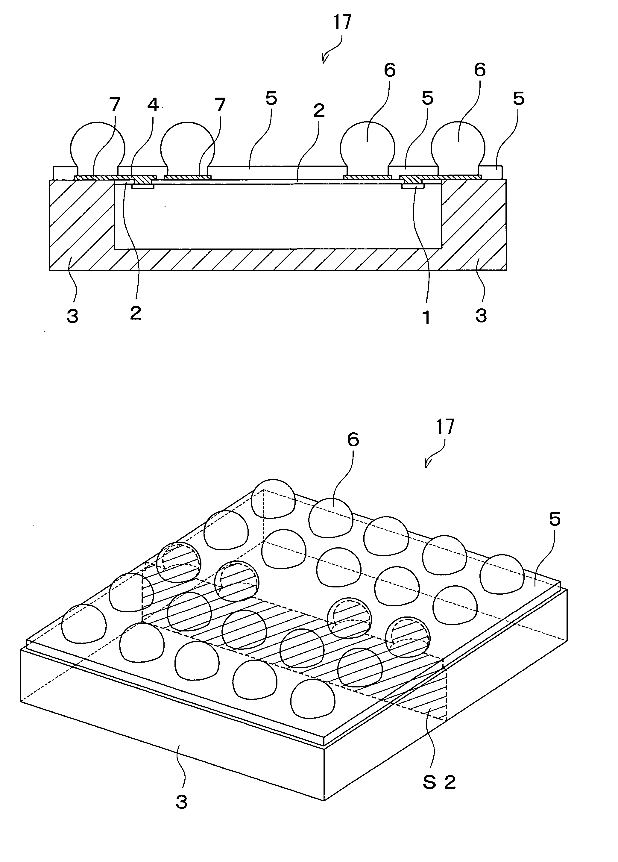
[0073] A second embodiment of the present invention will be described below with reference to FIGS. 7(a) and 7(b). For convenience of explanation, components having the same functions as those described in the first embodiment are given the same reference numerals, and no explanation will be given to the components. FIG. 7(b) is a perspective view of a semiconductor device 17 of the present embodiment. FIG. 7(a) is a cross-sectional view taken along surface S2 of FIG. 7(b).

[0074] As illustrated in FIG. 7(a), the semiconductor device 17 includes external connection terminals 6, respectively connected to the external connection pads 7, in addition to the arrangement of the semiconductor device 16 described in the first embodiment with reference to FIGS. 1(a) and 1(b). As the external connection terminals 6, spherical solder balls are used, for example. For example, the external connection terminals 6 are formed in the following manner. That is, the spherical solder balls are put on a...

third embodiment

[0077] A third embodiment of the present invention will be described below with reference to FIG. 8. For convenience of explanation, components having the same functions as those described in the first embodiment are given the same reference numerals, and no explanation will be given to the components.

[0078]FIG. 8 is a cross-sectional view of a semiconductor device 18 of the present embodiment. As illustrated in FIG. 8, the semiconductor device 18 is different from the semiconductor device 16 illustrated in FIG. 1(a) in that the surface of the semiconductor chip 10 opposite to the principal surface is exposed. The semiconductor device 18 is manufactured in the following manner. That is, after the protective resin 5 has been formed as described with reference to FIGS. 6(a) and 6(b), the sealing resin 3 covering the surface of the semiconductor chip 10 opposite to the principal surface is grinded with the use of a backgrinding machine (grinding step). The grinding may be carried out ...


PUM


Abstract

A semiconductor device includes: a semiconductor chip having a plurality of electrode pads formed on a principal surface thereof; a sealing resin, which covers both (i) side surfaces of the semiconductor chip and (ii) a surface of the semiconductor chip opposite to the principal surface; and external connection pads, which are provided on both (I) the principal surface and (II) a surface of the sealing resin flush with the principal surface, and which are electrically connected to the electrode pads. Thus, a semiconductor device is provided which makes it possible to place external connection pads at wider intervals, and which makes it possible to widen wires and to place the wires at wider intervals.

Description

[0001] This Nonprovisional application claims priority under 35 U.S.C. § 119(a) on Patent Application No. 014810 / 2005 filed in Japan on Jan. 21, 2005, the entire contents of which are hereby incorporated by reference. FIELD OF THE INVENTION [0002] The present invention relates to (i) a semiconductor device to be installed or incorporated in an electronic device and (ii) a method for manufacturing the semiconductor device. BACKGROUND OF THE INVENTION [0003] Portable devices have been miniaturized, upgraded, and thinned. Accordingly, there has been such a tendency that electronic parts to be installed in the devices are packaged at high density. Similarly, semiconductor IC packages have been required to be miniaturized and thinned. In order to keep pace with the miniaturization of the devices, a small package called CSP (chip size package) has been proposed. The CSP has a size equal or substantially equal to the size of a chip. [0004] Many types of CSP are formed in substantially the ...

Claims


Application Information

Patent Timeline
Patent Type & Authority Applications(United States)
IPC IPC(8): H01L23/48
CPCH01L21/561H01L21/568H01L21/6835H01L23/3114H01L23/5389H01L24/19H01L24/96H01L24/97H01L2221/68359H01L2224/04105H01L2224/20H01L2224/92H01L2224/97H01L2924/01013H01L2924/01029H01L2924/01078H01L2924/01079H01L2924/14H01L2924/15311H01L2224/96H01L2224/82H01L2924/01005H01L2924/01006H01L2924/01024H01L2924/01033H01L2224/12105H01L2924/18162H01L2224/023H01L2924/0001
Inventor NAKANISHI, HIROYUKIMORI, KATSUNOBU
Owner SHARP KK
Why Eureka
Try Eureka