

Method for manufacturing industrial products and combination of masks for manufacturing the same
a technology for industrial products and masks, applied in semiconductor/solid-state device testing/measurement, instruments, photomechanical equipment, etc., can solve the problems of increasing the difficulty in generating flawless masks with many fine lines and space patterns, short-circuit failure, and generation of interconnect pattern defects or element pattern defects
- Summary
- Abstract
- Description
- Claims
- Application Information
AI Technical Summary
Benefits of technology
Problems solved by technology
Method used
Image

Examples
Embodiment Construction
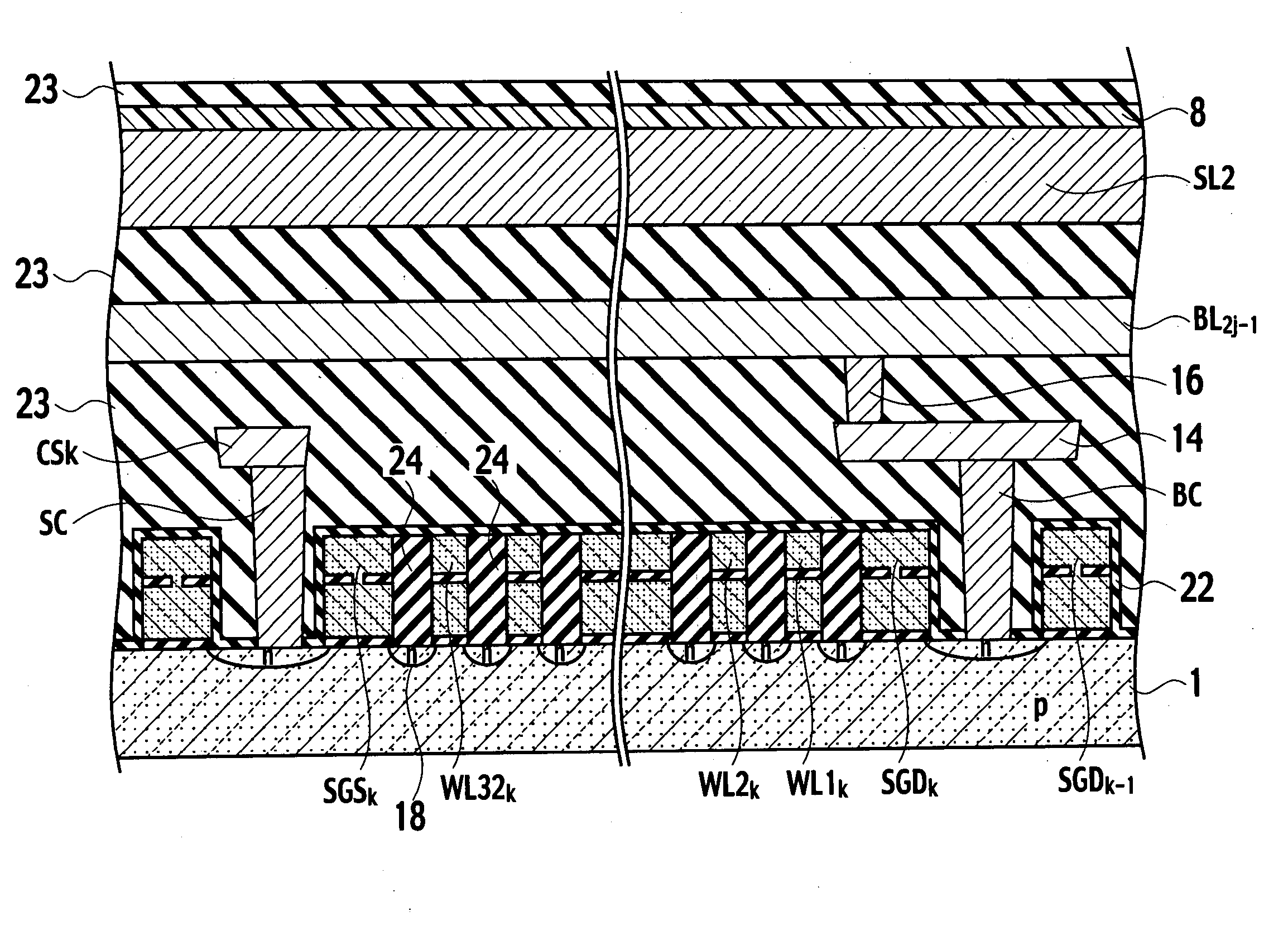
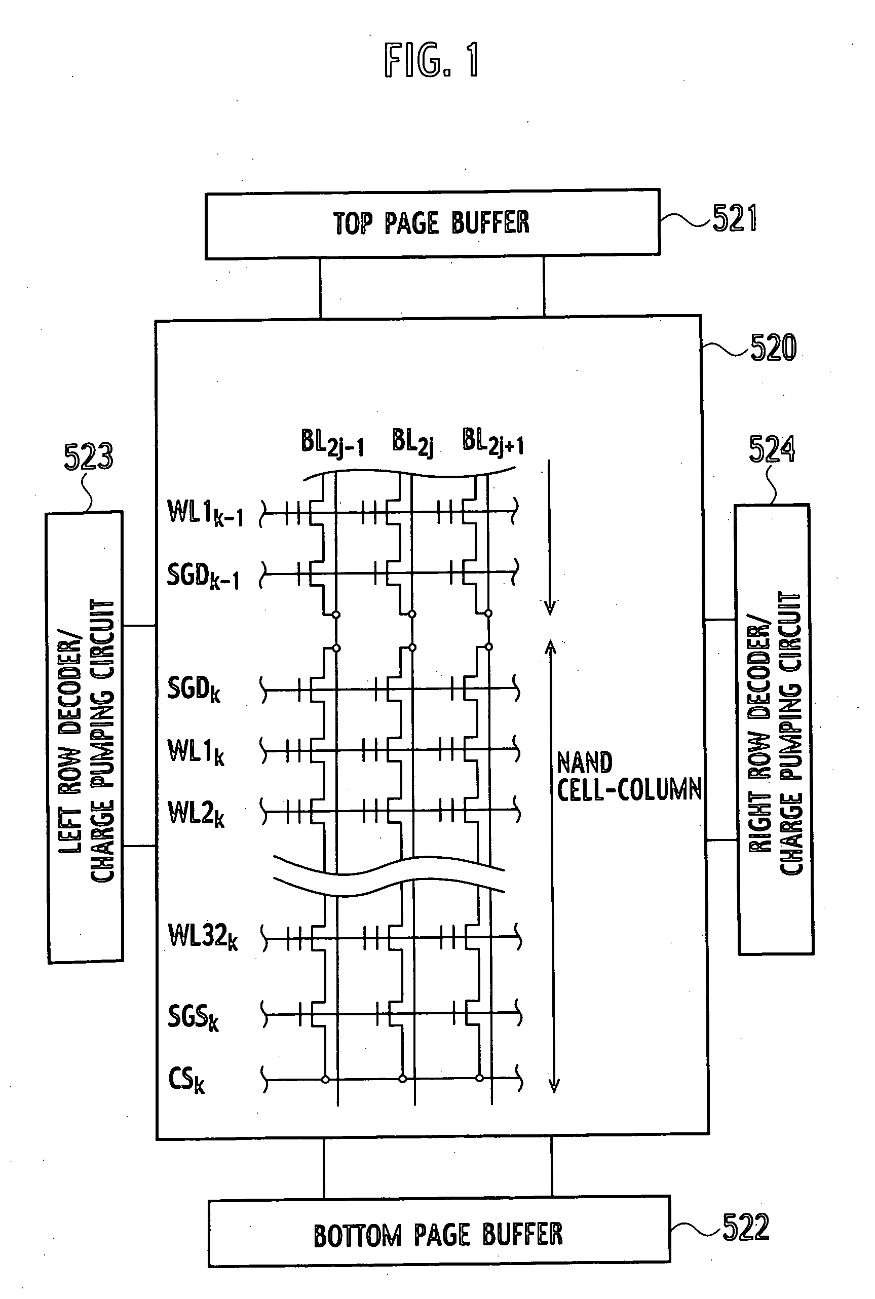
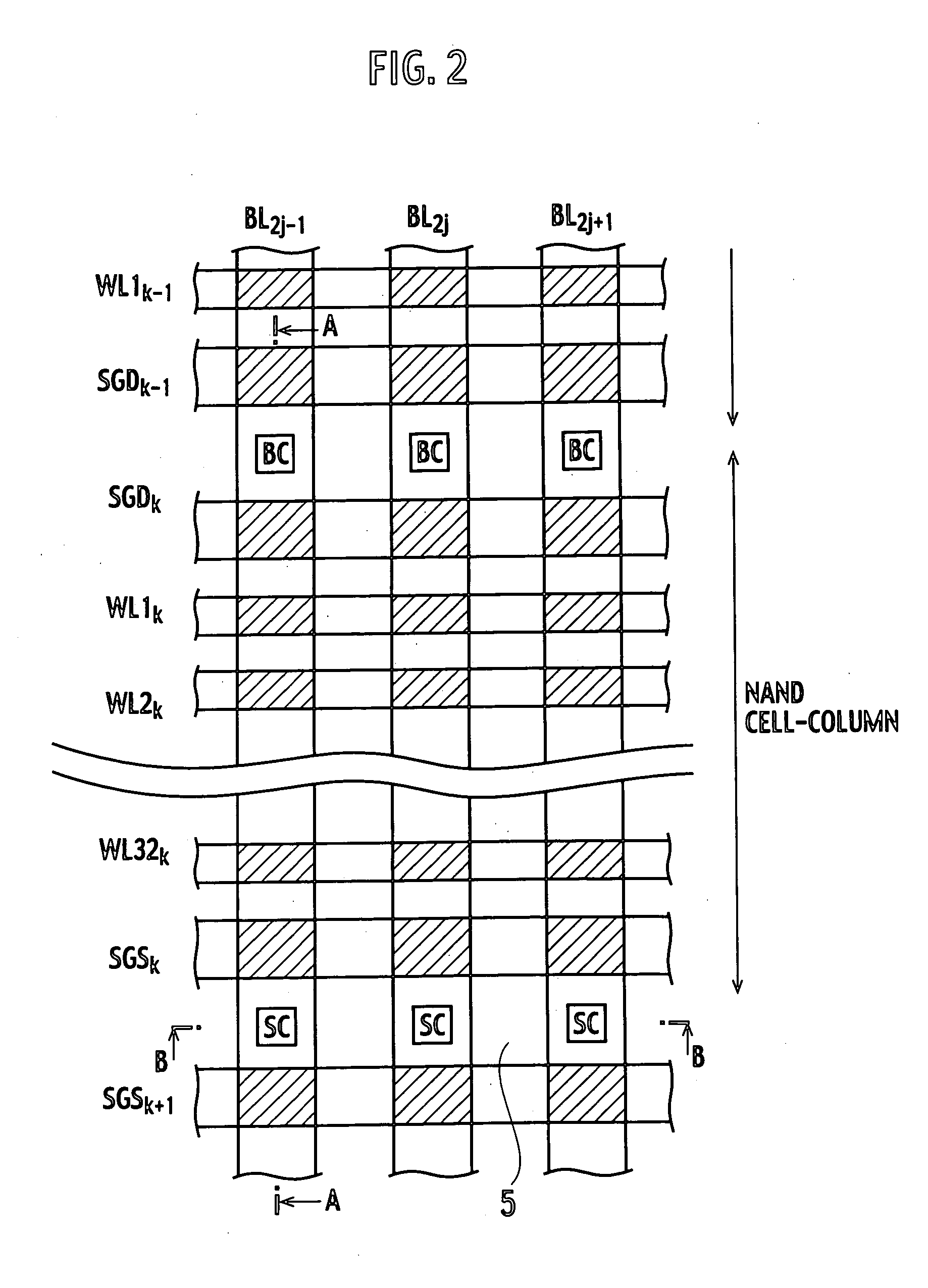
[0067] A technical idea of functioning as voltage-measuring patterns capable of detecting short-circuit failure or open-circuit failures by combining process-level evaluation patterns for verifying reliance of a target industrial product (final product) with various intermediate product patterns of the industrial product is exemplified in detail with the embodiment of the present invention given below using the accompanying drawings. Here, the intermediate product patterns correspond to actual device patterns, each of which implements at least a part of an intermediate product of the industrial product (final product), at a surface of a base body to be processed by a sequence of processes including lithography process with a working mask, the sequence of processes corresponds to a part of an entire procedure for manufacturing the industrial product.
[0068] Another technical idea facilitating employment of a defective mask, by electrically isolating a defective portion (if there is) ...
PUM
 Abstract
Description
Claims
Application Information