Novel monolithic, combo nonvolatile memory allowing byte, page and block write with no disturb and divided-well in the cell array using a unified cell structure and technology with a new scheme of decoder and layout

a nonvolatile memory and cell array technology, applied in the field of nonvolatile integrated circuit memory, can solve the problems of preventing the design of memory cells, affecting the performance of memory cells,

Inactive Publication Date: 2006-08-03
CALLAHAN CELLULAR L L C
View PDF36 Cites 7 Cited by
  • Summary
  • Abstract
  • Description
  • Claims
  • Application Information

AI Technical Summary

Benefits of technology

[0039] An object of this invention is to provide a nonvolatile memory array having a single transistor memory cell for incorporation as a Flash memory and a two transistor memory cell for incorporation as an EEPROM.
[0040] Another object of this invention is to provide a one-transistor Flash nonvolatile memory cell having a floating gate with a low coupling coefficient to permit a smaller memory cell.
[0041] A further objective of this invention is to provide a two-transistor EEPROM nonvolatile memory cell having a floating gate with a low coupling coefficient connected in series with a small select transistor to permit a smaller memory cell.
[0042] Further another object of this invention is to provide a memory array in which the Flash memory and EEPROM memory cells maybe integrated on the same substrate by using the same process technology.

Problems solved by technology

Nonvolatility requires the device to retain data without power applied for the lifetime of the application.
Both of the reliability requirements of endurance and data retention have associated failure rates, which must be minimized.
However, the “wings” prevent the design of the memory cell 10 from achieving a minimum size.

Method used


Image

  • Novel monolithic, combo nonvolatile memory allowing byte, page and block write with no disturb and divided-well in the cell array using a unified cell structure and technology with a new scheme of decoder and layout
  • Novel monolithic, combo nonvolatile memory allowing byte, page and block write with no disturb and divided-well in the cell array using a unified cell structure and technology with a new scheme of decoder and layout
  • Novel monolithic, combo nonvolatile memory allowing byte, page and block write with no disturb and divided-well in the cell array using a unified cell structure and technology with a new scheme of decoder and layout

Examples


Embodiment Construction

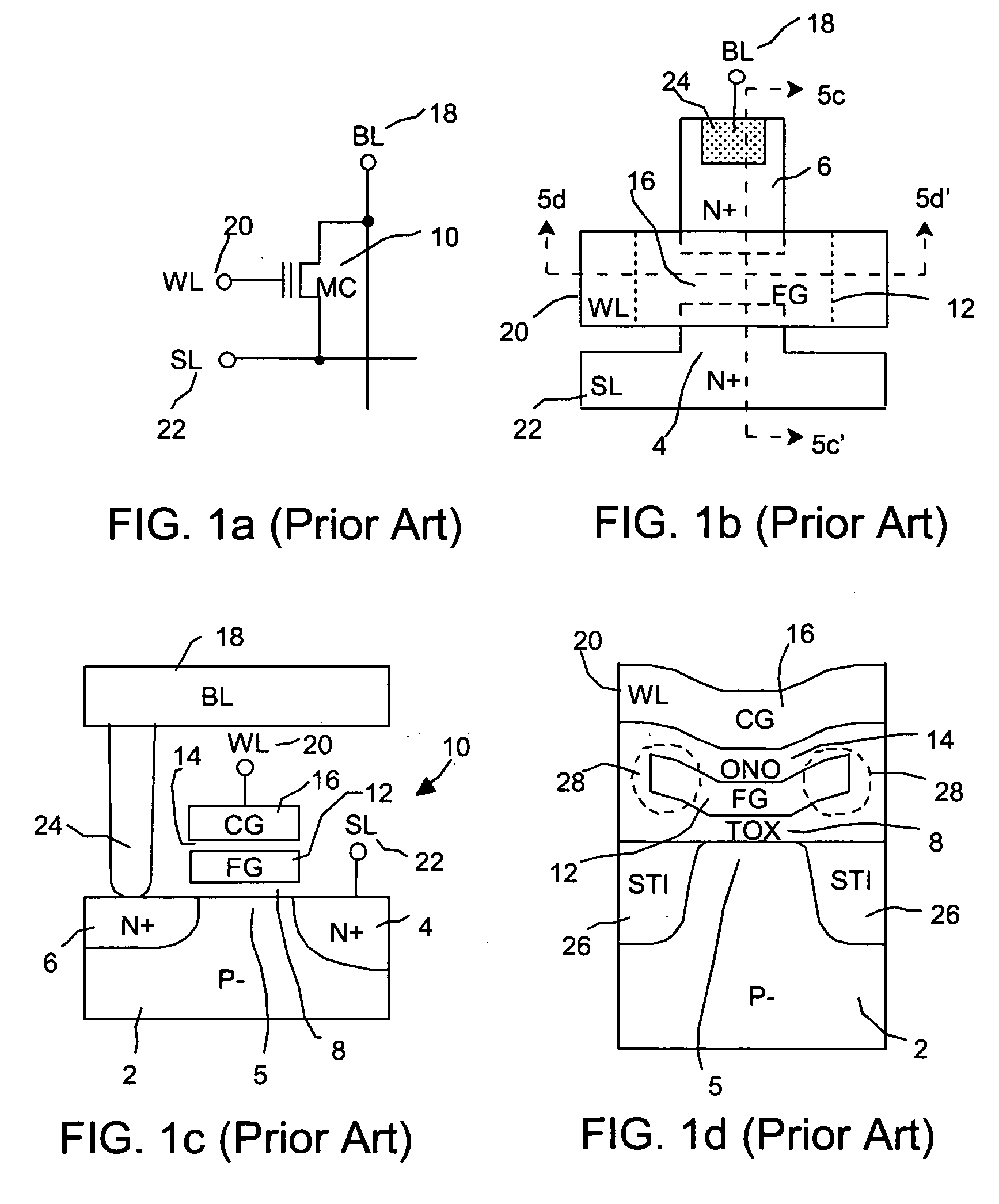
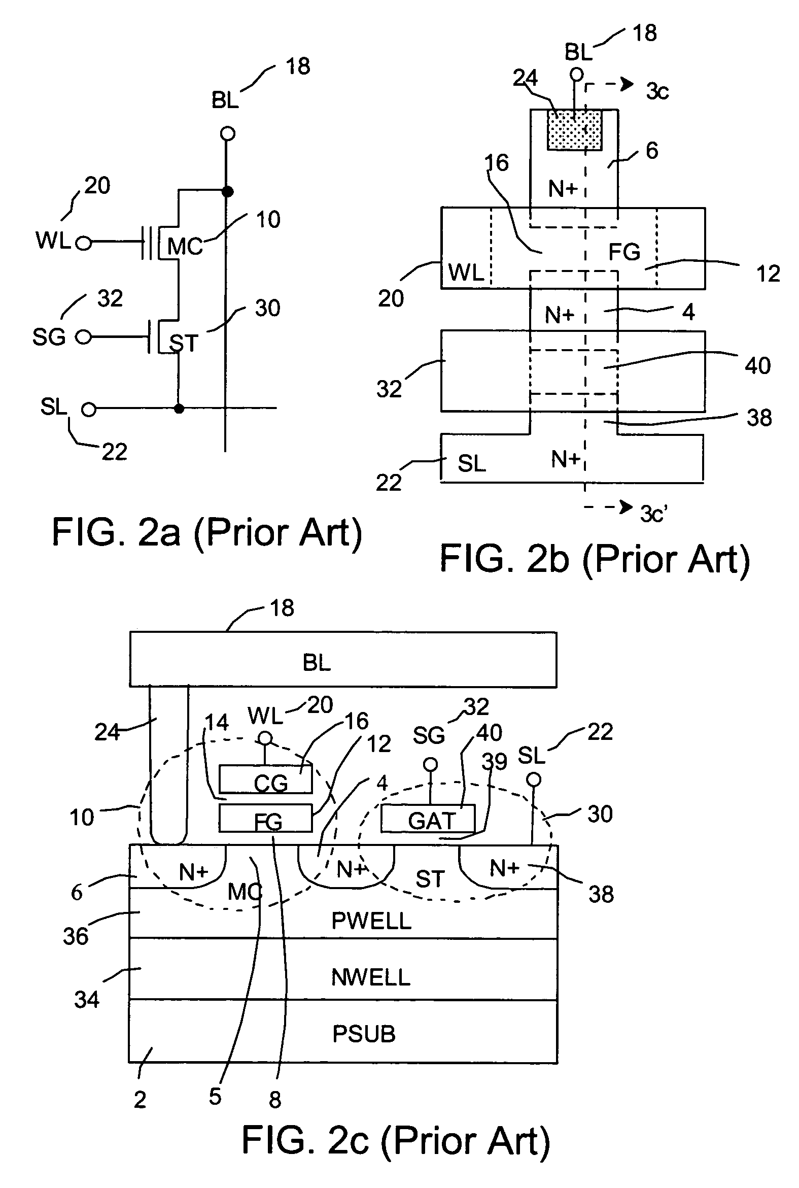
[0067] As described above the EEPROM nonvolatile memory is distinguished from the Flash memory in that the byte-alterable feature of the EEPROM is used to store the data code as opposed to the block (page or full chip) alterability of the Flash memory for storing program code. Since EEPROM is used for retaining information that is changed more often such as data, the EEPROM is subjected to more programming and erasing cycles in units of bytes and therefore, the EEPROM must have a higher endurance. In order to achieve high endurance of 1 million cycles, high-voltage bitline (program) and wordline (erase) disturbs to the non-selected bytes have to be eliminated during repeat program and erase operations. This has led to a two transistor EEPROM nonvolatile memory cell that is large and non-scalable but offers no bitline program disturb. In addition, the wordline of EEPROM cell array has been traditionally divided to avoid wordline erase disturb to the unselected bytes. Alternately, the...


PUM


Abstract

A nonvolatile memory array has a single transistor flash memory cell and a two transistor EEPROM memory cell which maybe integrated on the same substrate. The nonvolatile memory cell has a floating gate with a low coupling coefficient to permit a smaller memory cell. The floating gate placed over a tunneling insulation layer, the floating gate is aligned with edges of the source region and the drain region and having a width defined by a width of the edges of the source the drain. The floating gate and control gate have a relatively small coupling ratio of less than 50% to allow scaling of the nonvolatile memory cells. The nonvolatile memory cells are programmed with channel hot electron programming and erased with Fowler Nordheim tunneling at relatively high voltages.

Description

[0001] The present invention is a divisional application that claims priority under 35 U.S.C. §120 from U.S. patent application Ser. No. 10 / 351,180, filing date Jan. 4, 2003, now U.S. Pat. No. _______, issued ______; which is related to and claims benefit of priority of the filing date of U.S. Provisional Patent Application serial No. 60 / 394,202 filed on Jul. 5, 2002 and entitled “A Novel Monolithic Nonvolatile Memory Allowing Byte, Page and Block Write With No Disturb and Divided-Well in The Cell Array Using A Unified Cell Structure and Technology With A New Scheme of Decoder”, which is herein incorporated by reference; and which is further related to and claims benefit of priority of the filing date of U.S. Provisional Patent Application serial No. 60 / 426,614 filed on Nov. 14, 2002, entitled “A Novel Monolithic, Combo Nonvolatile Memory Allowing Byte, Page And Block Write With No Disturb And Divided-Well In The Cell Array Using A Unified Cell Structure And Technology With A New Sc...

Claims


Application Information

Patent Timeline
Patent Type & Authority Applications(United States)
IPC IPC(8): G11C16/04G11C16/10G11C16/14H01L21/8247H01L27/115
CPCG11C16/0408G11C16/0416G11C16/0433H01L27/11524G11C16/14H01L27/115H01L27/11521G11C16/10H10B41/35H10B69/00H10B41/30
Inventor LEE, PETER W.HSU, FU-CHANGTSAO, HSING-YAMA, HAN-REI
Owner CALLAHAN CELLULAR L L C
Why Eureka
Try Eureka