

Stage control apparatus and method, stage apparatus and exposure apparatus
a technology of stage apparatus and control system, applied in the field of stage control apparatus, can solve the problems of inability to follow the control system and inability to achieve the desired focusing ability
- Summary
- Abstract
- Description
- Claims
- Application Information
AI Technical Summary
Benefits of technology
Problems solved by technology
Method used
Image

Examples
first embodiment
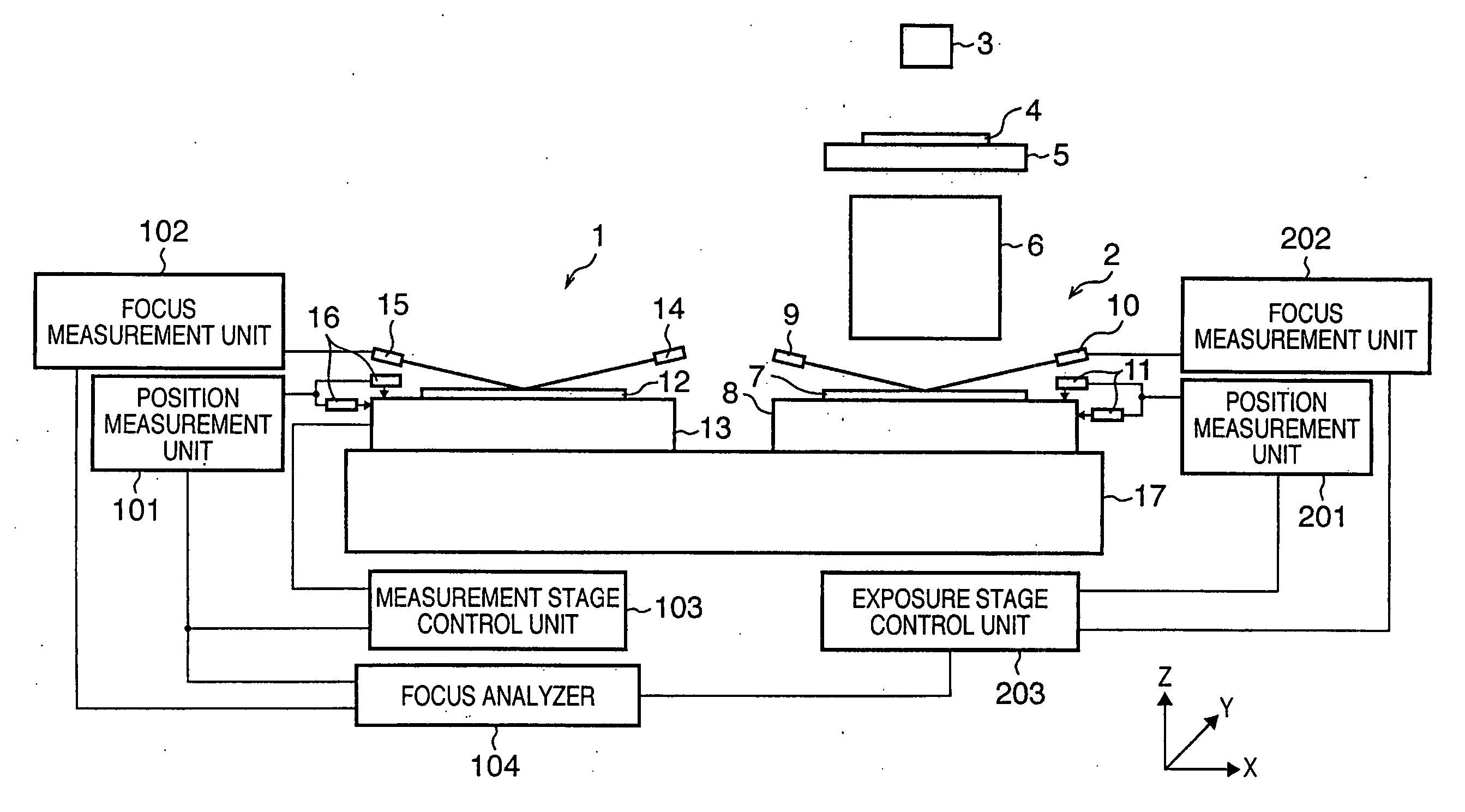
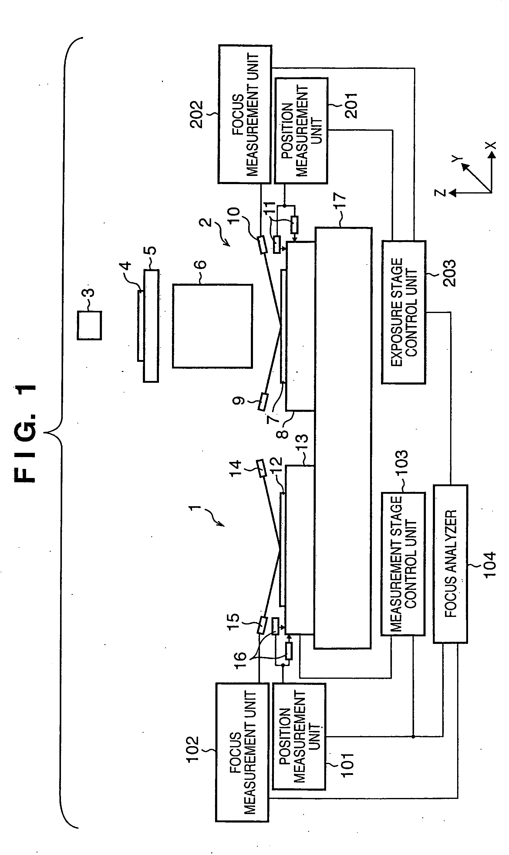
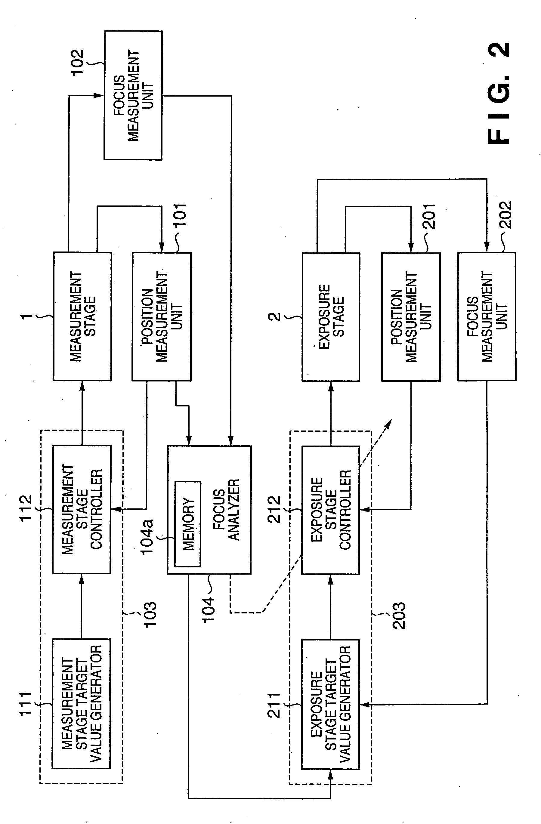
[0020]FIG. 1 is a diagram illustrating an overview of the structure of a semiconductor exposure apparatus according to a first embodiment of the present invention. As shown in FIG. 1, the exposure apparatus of this embodiment has twin stages, namely, a measurement stage system 1 and an exposure stage system 2. Components 101 to 104 that control the measurement stage system 1 and components 201 to 203 that control the exposure stage system 2 construct at least part of a stage controller.
[0021] The exposure stage system 2 has a wafer stage (referred to as an “exposure stage” below) 8 on which a wafer is placed and moved and with a structure for exposing the wafer. This structure is such that exposure light emitted from a light source 3 irradiates a reticle 4 that has been placed on a reticle stage 5. A projection optical system 6 narrows down the exposure light (reticle pattern light), which has passed through the reticle 4, at a prescribed magnification and projects the light upon t...
second embodiment
[0038]FIG. 5 is a block diagram illustrating the structure of the exposure stage controller 212 according to a second embodiment of the invention. In the second embodiment, the internal structure of the exposure stage controller 212 is changed from the arrangement shown in FIG. 3 to the arrangement shown in FIG. 5. Other aspects are the same as those of the first embodiment and need not be described again.
[0039] The arrangement of FIG. 5 includes a compensator 221, an integrator 222 and a state compensator 223. In the second embodiment, the arrangement is such that the compensator 221 has been added to a control system well known as a status feedback servo system. That is, the deviation signal between the target value from the exposure stage target value generator 211 and the vertical position of the stage output from the position measurement unit 201 is supplied from the arithmetic unit 215 to the integrator 222 and compensator 221 of a status feedback servo system. The integrator...
third embodiment
[0042]FIG. 6 is a diagram illustrating the configuration of a focus control system of a stage control apparatus in a semiconductor exposure apparatus according to a third embodiment of the present invention. In the first and second embodiments, the measurement stage system 1 is provided to measure flatness, wafer by wafer, and to obtain a spatial frequency value of the target position. In the third embodiment, the spatial frequency value of the target position of every wafer is held in a wafer database to make utilization possible by the exposure stage system 2 and to enable the deletion of the measurement stage system 1 shown in FIG. 1.
[0043] Components in FIG. 6 similar to those in FIGS. 1 and 2 are designated by like reference characters and need not be described again. The arrangement of FIG. 6 includes the focus measurement unit 202 for measuring the vertical coordinate value of the surface of a wafer placed on a stage, a wafer discriminator 61 for discriminating a wafer place...
PUM
 Abstract
Description
Claims
Application Information