Inductive plasma system with sidewall magnet

a sidewall magnet and plasma technology, applied in plasma techniques, coatings, contact material materials, etc., can solve the problems of inconsistencies in device performance, poor gapfill ability, and difficult to completely fill high-aspect-ratio gaps using conventional cvd techniques, and achieve the effect of improving uniformity

a sidewall magnet and plasma technology, applied in plasma techniques, coatings, contact material materials, etc., can solve the problems of inconsistencies in device performance, poor gapfill ability, and difficult to completely fill high-aspect-ratio gaps using conventional cvd techniques, and achieve the effect of improving uniformity

US20060177600A1Inactive Publication Date: 2006-08-10APPLIED MATERIALS INC

Image

  • Inductive plasma system with sidewall magnet
  • Inductive plasma system with sidewall magnet
  • Inductive plasma system with sidewall magnet

Examples


Embodiment Construction

1. Overview

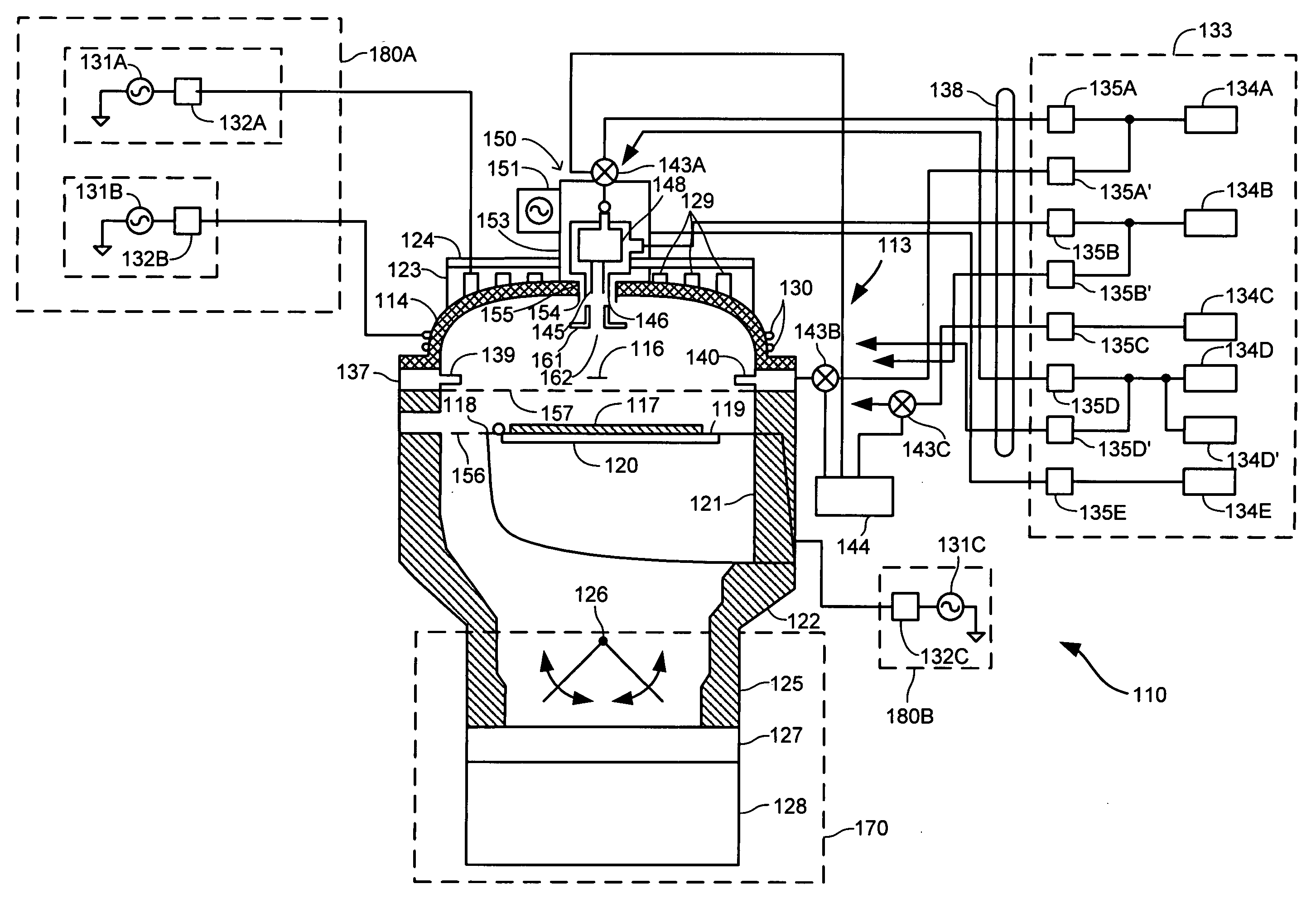
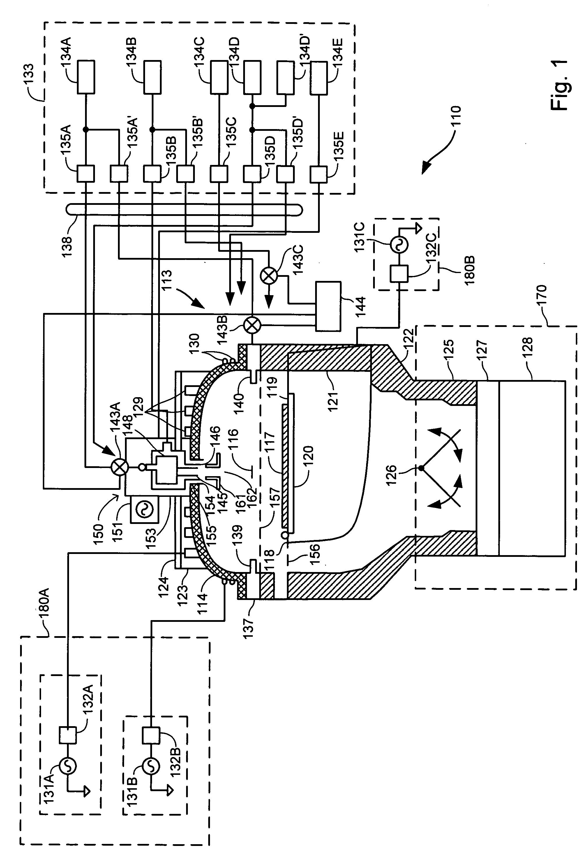
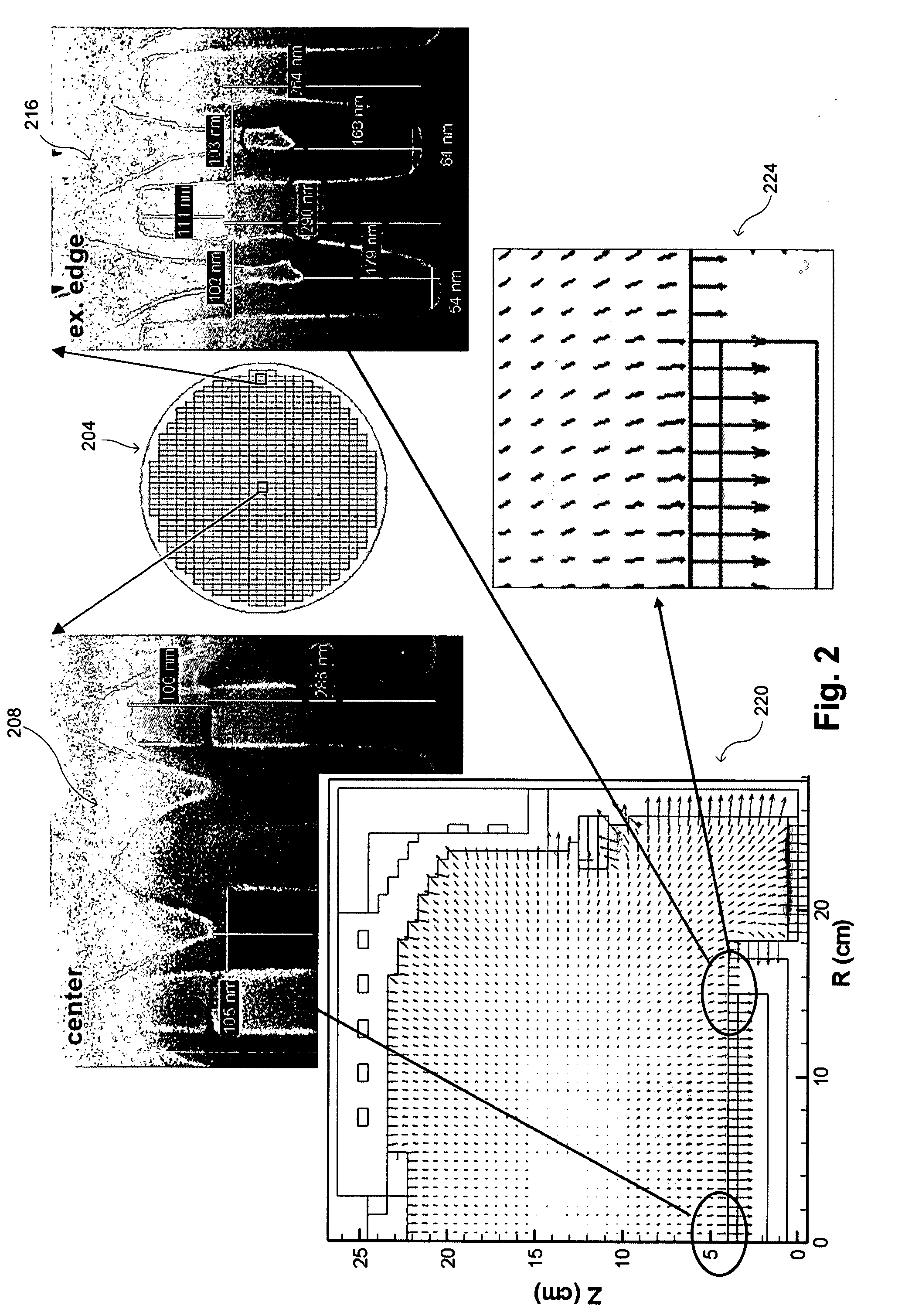
[0019] Embodiments of the invention provide an ICP reactor that uses a magnetic field generated by a magnetic confinement ring to control the distribution of ionic species within the chamber. When the inventors were initially confronted with the problem of improving deposition uniformity, they began by considering a number of different sources for nonuniformities and undertook a variety of studies to understand how these sources contributed to the resultant nonuniformity. These studies included both simulation and experimental studies. In particular, three principal classes of factors were identified as bearing on uniformity characteristics: plasma characteristics, chamber flow distributions, and thermal effects.

[0020] For example, in gapfill applications, better overall gapfill is achieved with higher ion densities in the plasma. Similarly, improved center-to-edge uniformity across a wafer is achieved when the ion distribution in the chamber has better uniformity. One...


PUM

PropertyMeasurementUnit
Magnetic fieldaaaaaaaaaa
Poweraaaaaaaaaa

Abstract

A substrate processing system has a housing that defines a process chamber. A substrate holder is disposed within the process chamber and configured to support a substrate within a substrate plane during substrate processing. A gas-delivery system is configured to introduce a gas into the process chamber. A pressure-control system maintains a selected pressure within the process chamber. A high-density-plasma generating system is operatively coupled with the process chamber. A magnetic confinement ring with magnetic dipoles is disposed circumferentially around a symmetry axis orthogonal to the substrate plane and provides a magnetic field with a net dipole moment substantially nonparallel with the substrate plane. A controller controls the gas-delivery system, the pressure-control system, and the high-density plasma system.

Description

BACKGROUND OF THE INVENTION [0001] One of the primary steps in the fabrication of modern semiconductor devices is the formation of a film, such as a silicon oxide film, on a semiconductor substrate. Silicon oxide is widely used as an insulating layer in the manufacture of semiconductor devices. As is well known, a silicon oxide film can be deposited by a thermal chemical-vapor deposition (“CVD”) process or by a plasma-enhanced chemical-vapor deposition (“PECVD”) process. In a conventional thermal CVD process, reactive gases are supplied to a surface of the substrate, where heat-induced chemical reactions take place to produce a desired film. In a conventional plasma-deposition process, a controlled plasma is formed to decompose and / or energize reactive species to produce the desired film. [0002] Semiconductor device geometries have decreased significantly in size since such devices were first introduced several decades ago, and continue to be reduced in size. This continuing reducti...

Claims


Application Information

Patent Timeline
10 Aug 2006
Publication
US20060177600A1
IPC
H05H1/02; C23C16/00; H05H1/46
CPC
H01J37/321; H01J37/32688; H01R4/66; H02G13/80
Inventors
LU, SIQING; LIANG, QIWEI