Metal and metal oxide patterned device

Inactive Publication Date: 2006-08-17
EASTMAN KODAK CO
View PDF19 Cites 39 Cited by
  • Summary
  • Abstract
  • Description
  • Claims
  • Application Information

AI Technical Summary

Benefits of technology

[0012] The invention provides flexible conductive patterned substrate with a low vapor transmission rate and transparent non-conductive regions.

Problems solved by technology

This method does create a metallic pattern, but uses many steps with undesirable, reactive chemistries and does not have metal oxide in the non-metal areas to improve vapor and moisture properties of the film.

Method used


Image

  • Metal and metal oxide patterned device
  • Metal and metal oxide patterned device
  • Metal and metal oxide patterned device

Examples


example

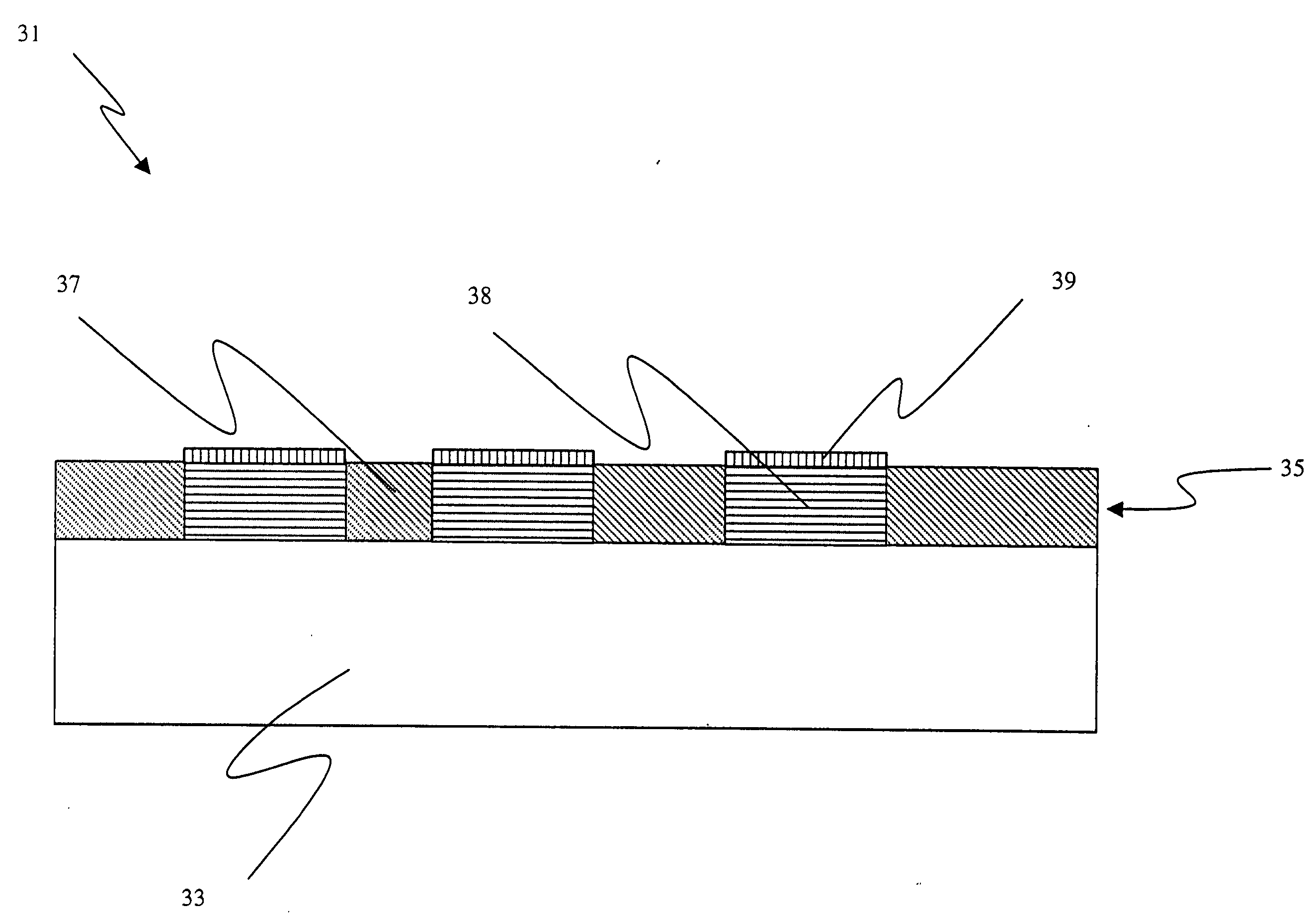
[0058] A flexible, biaxially oriented PET film was used as the substrate for the patterned device. It was approximately 100 micrometers thick PET film known commercially as Estar with a transmission of 81%. The substrate was then coated with aluminum. A DC magnetron sputter gun was used to deposit 700 angstroms of aluminum onto the substrate. The sputtering was done at 5 mT in an argon atmosphere.

[0059] The aluminum coated piece of PET was then patterned with a simple circuit design with a commercially available solvent-based ink commercially available as Sharpie® permanent black marker. The ink consisted of dyes in a solvent solution of n-propanol (71-23-8), n-butanol (71-36-3) and diacetone alcohol (123-42-2). Once the ink was dry the sample was immersed into a water bath at 90° C. for 1 minute. The time was sufficient to convert the unmasked area to aluminum oxide. Once the conversion was complete, the ink was removed by rinsing the surface with acetone. The resulting patterned ...


PUM


Abstract

The invention relates to a patterned device comprising a substrate covered by a pattern of metal and oxidized metal surrounding said pattern of metal.

Description

FIELD OF THE INVENTION [0001] This invention relates to a patterned aluminum and aluminum oxide layer on a substrate, and more particularly relates to a method for forming such a pattern by the selective oxidation of an aluminized web which results in a web covered with aluminum and aluminum oxide in which the pattern of the aluminum is determined by the application of a hydrophobic ink. BACKGROUND OF THE INVENTION [0002] Thin patterned films of metal on flexible substrates are useful for many applications. They are especially required for producing inexpensive flexible circuits and also find use in optical films and electronic display devices. [0003] One of the least expensive ways of generating a thin flexible patterned aluminum substrate is to start with an aluminized web and then selectively remove the aluminum from the web. Typically this is done by patterning a resist onto the web and then etching the resist free areas or by depositing a caustic etch in the negative of the des...

Claims


Application Information

Patent Timeline
IPC IPC(8): H01L21/44
CPCH05K1/0393H05K1/09H05K3/02H05K2201/0108H05K2203/0315H05K2203/1142
Inventor BRUYNS, ROLAND C.BRICKEY, CHERYL J.BOURDELAIS, ROBERT P.PALMERI, JOHN M.
Owner EASTMAN KODAK CO
Why Eureka
Try Eureka