Semiconductor device and manufacturing method thereof

Inactive Publication Date: 2006-08-24
TERAMIKROS INC
View PDF7 Cites 28 Cited by
  • Summary
  • Abstract
  • Description
  • Claims
  • Application Information

AI Technical Summary

Benefits of technology

[0007] It is an object of this invention to provide a semiconductor device and a manufacturing method thereof capable of preventing cracks from being easily caused in a rear surface of a semiconductor substrate.
[0010] According to this semiconductor device, the rear surface of the semiconductor substrate is a rough surface having a height difference of 1 to 5 μm, and this ensures that the rough surface can be covered with the protective film, thereby making it possible to prevent the cracks from being easily caused in the rear surface of the semiconductor substrate.

Problems solved by technology

However, if a semiconductor substrate in a wafer state is made too thin, the semiconductor substrate is damaged in a semiconductor manufacturing process in which integrated circuits are formed on a front surface of the semiconductor substrate in the wafer state.
In the semiconductor device obtained by the conventional manufacturing method described above, the rear surface of the semiconductor substrate is ground to form minute and acutely-angled irregularities on the rear surface of the semiconductor substrate, so that even if a protective film made of a resin is formed on the minute and acutely-angled irregular surface, it is difficult to ensure that the resin is filled into the inner part of the minute and acutely-angled concave portions.
As a result, there is a problem that cracks may be caused in the rear surface of the semiconductor substrate due to the fact that the inner parts of the minute and acutely-angled concave portions are not covered with the protective film.

Method used


Image

  • Semiconductor device and manufacturing method thereof
  • Semiconductor device and manufacturing method thereof
  • Semiconductor device and manufacturing method thereof

Examples


first embodiment

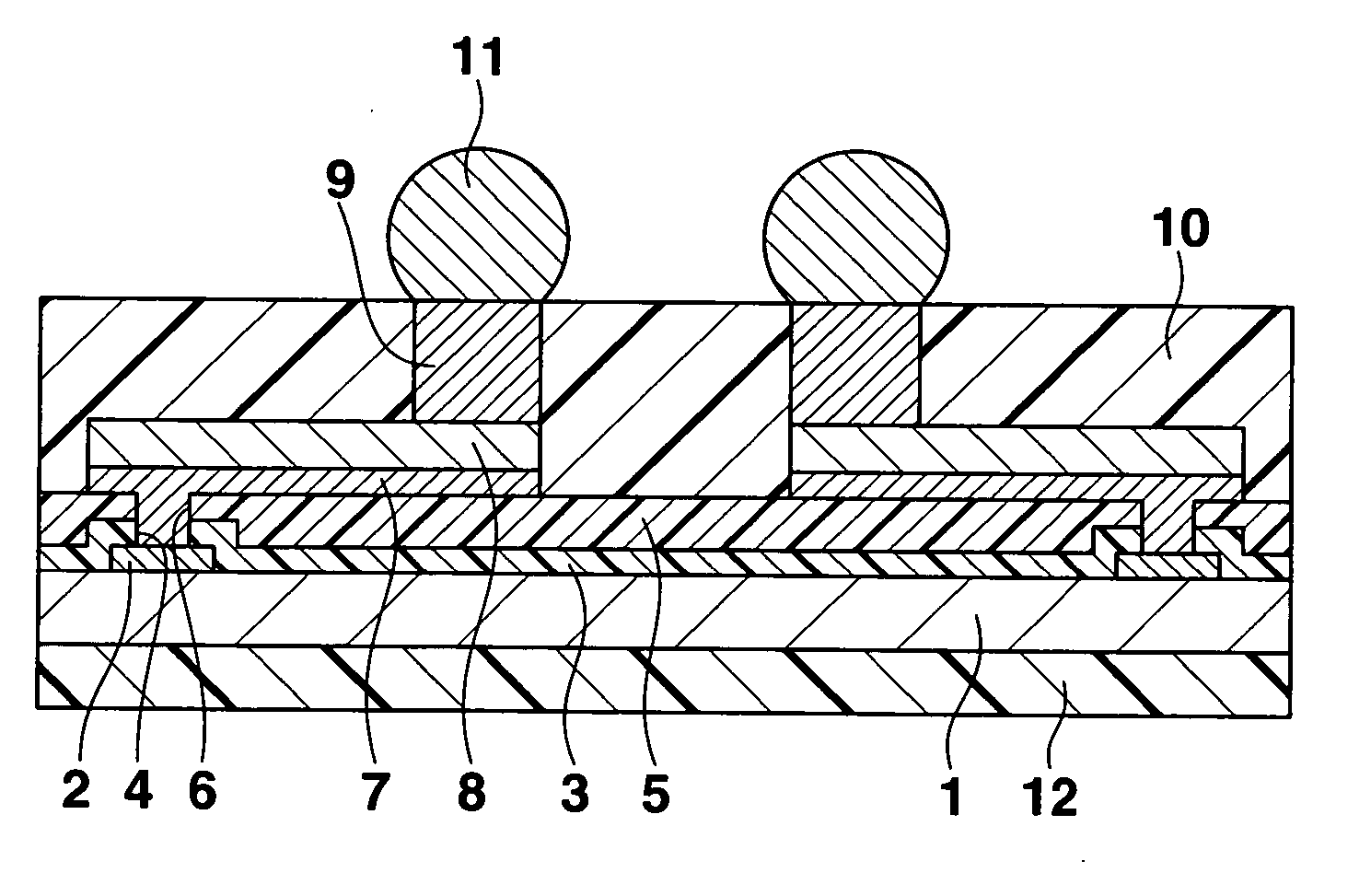
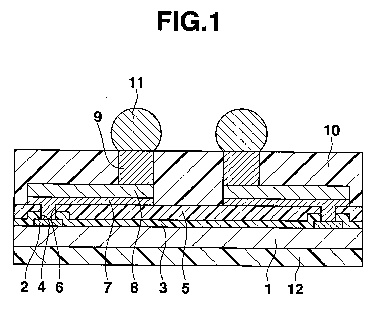
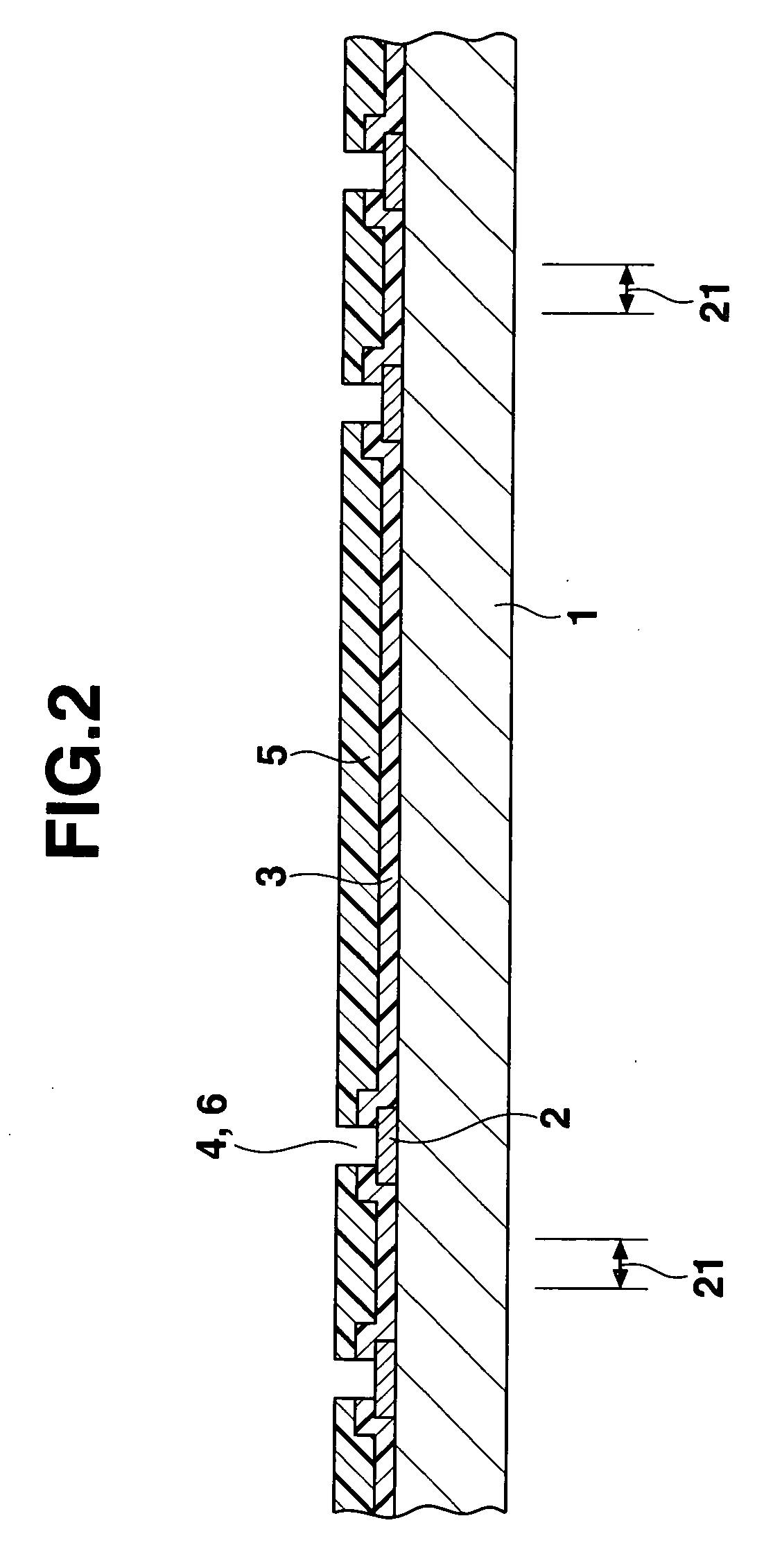
[0039]FIG. 1 shows a sectional view of a semiconductor device as a first embodiment of the invention. The semiconductor device is generally called a chip size package (CSP), and has a silicon substrate (semiconductor substrate) 1. An integrated circuit (not shown) having a predetermined function is provided on an upper surface of the silicon substrate 1. A plurality of connection pads 2 made of an aluminum-based metal or the like are provided on the periphery of the upper surface of the substrate in such a manner as to be connected to the integrated circuit.

[0040] An insulating film 3 made of silicon oxide or the like is provided on the upper surface of the silicon substrate 1 except for the center of the respective connection pad 2, so that the center of the connection pad 2 is exposed via an opening 4 provided in the insulating film 3. A protective film 5 made of an epoxy-based resin, a polyimide-based resin or the like is provided on an upper surface of the insulating film 3. In...

second embodiment

[0057]FIG. 14 shows a second embodiment of this invention. An integrated circuit (not shown) having a predetermined function is provided on an upper surface of a silicon substrate 1, and a plurality of connection pads 2 made of an aluminum-based metal or the like are provided on the periphery of the upper surface in such a manner as to be connected to the integrated circuit.

[0058] An insulating film 3 made of silicon oxide or the like is provided on the upper surface of the silicon substrate 1, and the connection pads 2 so that the center of each connection pad 2 is exposed via an opening 4 provided in the insulating film 3. A protective film 5 made of an epoxy-based resin, a polyimide-based resin or the like is provided on an upper surface of the insulating film 3. In this case, an opening 6 is provided in the protective film 5 in a part corresponding to the opening 4 of the insulating film 3.

[0059] Foundation metal layers 7 made of copper or the like are provided on an upper sur...


PUM

PropertyMeasurementUnit
Heightaaaaaaaaaa
Thicknessaaaaaaaaaa
Semiconductor propertiesaaaaaaaaaa

Abstract

A semiconductor device includes a semiconductor substrate which has an integrated circuit formed on a front surface thereof, and a rough surface with a height difference of 1 to 5 μm on a rear surface thereof. A protective film is provided on the rear surface of the semiconductor substrate.

Description

CROSS-REFERENCE TO RELATED APPLICATIONS [0001] This application is based upon and claims the benefit of priority from prior Japanese Patent Applications No. 2005-043738, filed Feb. 21, 2005; and No. 2005-043739, filed Feb. 21, 2005, the entire contents of both of which are incorporated herein by reference. BACKGROUND OF THE INVENTION [0002] 1. Field of the Invention [0003] This invention relates to a semiconductor device and a manufacturing method thereof. [0004] 2. Description of the Related Art [0005] There has been a demand for thinner semiconductor devices as electronic equipment becomes thinner. However, if a semiconductor substrate in a wafer state is made too thin, the semiconductor substrate is damaged in a semiconductor manufacturing process in which integrated circuits are formed on a front surface of the semiconductor substrate in the wafer state. Thus, a technique has been developed wherein after the integrated circuits are formed on the front surface of the semiconducto...

Claims


Application Information

Patent Timeline
IPC IPC(8): H01L23/48
CPCH01L21/561H01L2224/0401H01L24/11H01L24/12H01L24/94H01L24/96H01L2224/0231H01L2224/1147H01L2224/13099H01L2224/16H01L2224/274H01L2924/01013H01L2924/01022H01L2924/01029H01L2924/01078H01L2924/01005H01L2924/01033H01L2924/014H01L23/3114H01L24/02H01L24/03H01L24/05H01L24/13H01L2224/02313H01L2224/02377H01L2224/05008H01L2224/05124H01L2224/05147H01L2224/05166H01L2224/05569H01L2224/05647H01L2224/13024H01L2224/94H01L2924/0001H01L2924/14H01L2924/3511H01L2924/00H01L2924/00014H01L2224/02F21S2/00F21V17/10F21V23/02F21V3/062
Inventor WAKABAYASHI, TAKESHIMIHARA, ICHIRO
Owner TERAMIKROS INC
Why Eureka
Try Eureka