
Board assembly, ink-jet and manufacturing method therefor

a technology of inkjet printing and assembly, which is applied in the direction of manufacturing tools, electrical apparatus contruction details, and manufacturing apparatuses, etc., can solve the problems of forming voids in the tin plate, increasing manufacturing costs, etc., and achieves the effect of preventing the increase of manufacturing costs, reducing electrical resistance between the circuit board and the other board or the piezoelectric actuator

Active Publication Date: 2006-08-24
BROTHER KOGYO KK
View PDF4 Cites 6 Cited by
  • Summary
  • Abstract
  • Description
  • Claims
  • Application Information

AI Technical Summary

Benefits of technology

[0009] An object of the present invention is to provide a method for manufacturing a board assembly that includes a circuit board, an electronic component mounted on the circuit board, and another board bonded to the circuit board, by which the board assembly having a decreased electrical resistance between boards can be manufactured relatively easily at a lowered cost.
[0010] Another object of the present invention is to provide a method for manufacturing an ink-jet head that includes a circuit board, a driver IC mounted on the circuit board, and a piezoelectric actuator bonded to the circuit board, by which the ink-jet head having a decreased electrical resistance between the circuit board and the piezoelectric actuator can be manufactured relatively easily at a lowered cost.
[0011] Still another object of the present invention is to provide a board assembly including a circuit board, an electronic component mounted on the circuit board, and another board bonded to the circuit board, which has a decreased electrical resistance between the boards and can be manufactured relatively easily at a lowered cost.
[0012] Still another object of the present invention is to provide an ink-jet head including a circuit board, a driver IC mounted on the circuit board, and a piezoelectric actuator bonded to the circuit board, which has a decreased electrical resistance between the circuit board and the piezoelectric actuator and can be manufactured relatively easily at a lowered cost.
[0017] In the first to fourth aspects, heating of the circuit board causes copper and tin to be scattered in the surface of the copper-made second terminal, to form a copper-tin alloy layer on the surface of the second terminal. This can relieve a problem that tin ions existing in the tin-plated layer formed on the surface of the second terminal are scattered over the conductive adhesive to thereby increase the electrical resistance between the second terminal of the circuit board and the terminal of the another board or the piezoelectric actuator, though this problem may occur if the tin-plated layer formed on the surface of the second terminal is bonded through a thermosetting conductive adhesive to the terminal of the another board or the piezoelectric actuator. That is, the electrical resistance between the circuit board and the another board or the piezoelectric actuator becomes lower.
[0018] In the plating step, there is no need to cover the second terminal against the tin plate. Thus, complicated procedures including a step of covering the second terminal and a step of removing the covering are not required, to prevent increase of a manufacturing cost.

Problems solved by technology

As a result, when the terminals of the FPC to be bonded to the piezoelectric actuator and the surface electrodes of the piezoelectric actuator are bonded with a conductive adhesive, tin ions existing in the tin that is plated on the terminals of the FPC are scattered over the conductive adhesive, thus forming voids within the tin plate.
In this case, however, complicated procedures including a step of covering the terminals and a step of removing the covering are required, and thus a manufacturing cost increases.

Method used


Image

  • Board assembly, ink-jet and manufacturing method therefor
  • Board assembly, ink-jet and manufacturing method therefor
  • Board assembly, ink-jet and manufacturing method therefor

Examples


Embodiment Construction

[0034] In the following, a preferred embodiment of the present invention will be described with reference to the accompanying drawings.

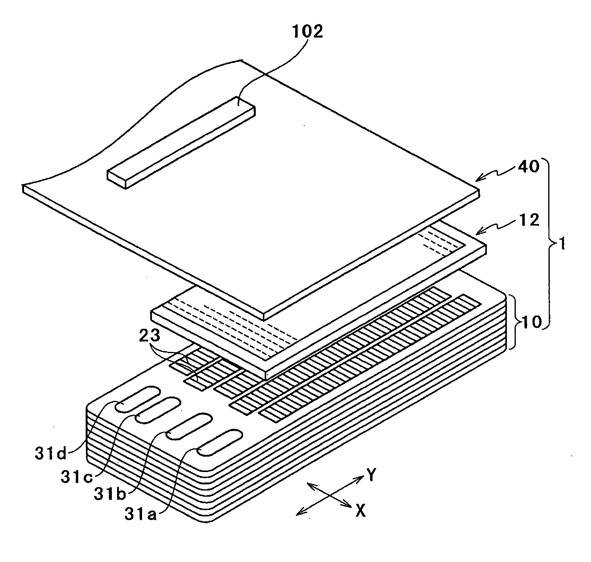
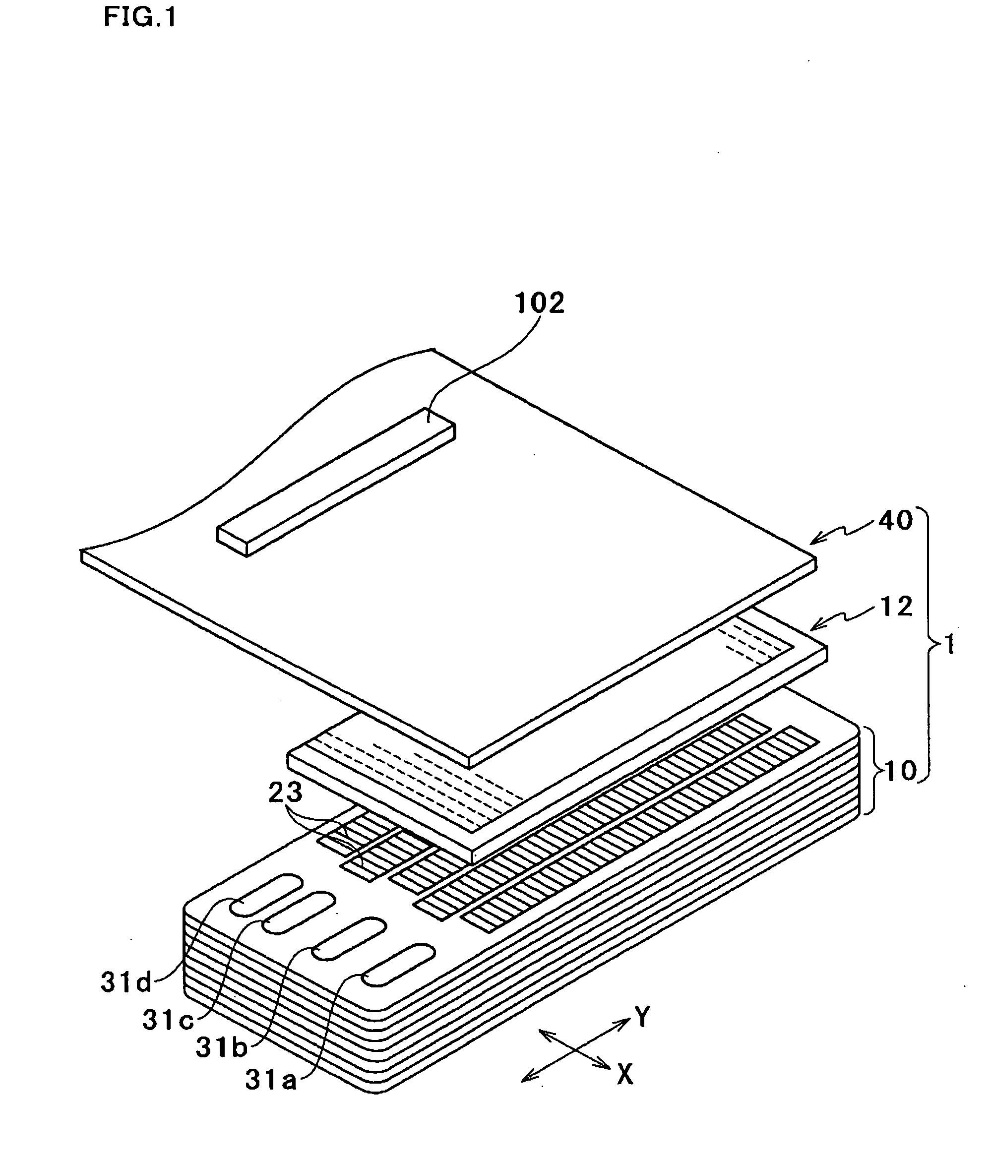
[0035] As shown in FIG. 1, an ink-jet head 1 of this embodiment includes a passage unit 10, a piezoelectric actuator 12, and an FPC 40. The head 1 is of so-called serial type, and mounted on a carriage (not illustrated) that reciprocates along a main scanning direction indicated by arrow X (hereinafter referred to as X direction) which is perpendicular to a paper conveyance direction or sub scanning direction indicated by arrow Y (hereinafter referred to as Y direction). The carriage accommodates removable ink cartridges respectively containing cyan ink, magenta ink, yellow ink, and black ink, which are fed to the head 1.

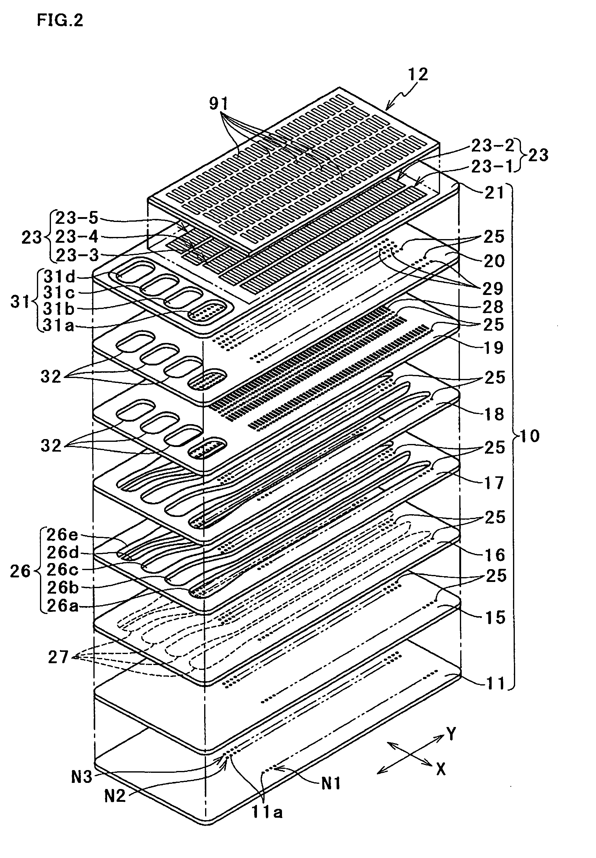
[0036] Many nozzles 11a (see FIG. 2), which open in a lower face of the passage unit, respectively communicates with the pressure chambers 23 formed in an upper face of the passage unit 10. In order to eject ink from a nozzle 11a, ...


PUM

PropertyMeasurementUnit
thicknessaaaaaaaaaa
diameteraaaaaaaaaa
lengthaaaaaaaaaa

Abstract

A method for manufacturing a board assembly comprises the steps of: tin-plating a first terminal and a copper-made second terminal that are formed on a circuit board; mounting an electronic component on the circuit board by means of gold-tin eutectic bonding between a gold electrode of the electronic component and the tin-plated first terminal; forming a copper-tin alloy on a surface of the second terminal by heating the circuit board after the mounting step; and bonding the second terminal having the copper-tin alloy formed on its surface to a terminal of another board by means of a thermosetting conductive adhesive.

Description

BACKGROUND OF THE INVENTION [0001] 1. Field of the Invention [0002] The present invention relates to a board assembly that includes a circuit board, an electronic component mounted on the circuit board, and another board bonded to the circuit board, to an ink-jet head that includes a circuit board, a driver IC mounted on the circuit board, and a piezoelectric actuator bonded to the circuit board, and also to a method for manufacturing them. [0003] 2. Description of Related Art [0004] Some ink-jet heads include a passage unit in which many pressure chambers are formed, and a piezoelectric actuator that has active portions corresponding to the respective pressure chambers and is bonded to the passage unit. Surface electrodes corresponding to the respective active portions are provided on an upper face of the piezoelectric actuator. Terminals of a flexible printed circuit (FPC) for applying voltage to the piezoelectric actuator are bonded to the respective surface electrodes. The FPC i...

Claims


Application Information

Patent Timeline
Patent Type & Authority Applications(United States)
IPC IPC(8): H05K7/08H05K7/06H05K7/02H05K7/10
CPCB41J2/14209B41J2/1609B41J2/1623B41J2/1643B41J2002/14217B41J2002/14225B41J2002/14459B41J2002/14491H01L24/83H01L2224/83801H01L2924/01005H01L2924/01009H01L2924/01015H01L2924/01029H01L2924/01047H01L2924/0105H01L2924/01078H01L2924/01079H01L2924/01082H01L2924/01322H01L2924/0781H05K1/189H05K3/244H05K3/321H05K3/3463H05K3/361H05K2201/10674H05K2203/1105H01L24/29H01L2224/2919H01L2924/01006H01L2924/01033H01L2924/0665H01L2924/0132H01L2224/2929H01L2224/29339H01L2224/29111H01L2924/00013Y10T29/49179Y10T29/49401Y10T29/49149Y10T29/42Y10T29/49144H01L2924/00H01L2924/00014H01L2224/29099H01L2224/29199H01L2224/29299H01L2924/181H01L2924/14
Inventor IMAI, KOJISHINKAI, YUJI
Owner BROTHER KOGYO KK
Learn More