Self-aligned semiconductor contact structures and methods for fabricating the same

a self-aligning, semiconductor technology, applied in semiconductor devices, semiconductor/solid-state device details, electrical apparatus, etc., can solve the problems of undesired electrical bridging, and affecting the electrical performance of the gate electrod

Inactive Publication Date: 2006-08-31
SAMSUNG ELECTRONICS CO LTD
View PDF8 Cites 9 Cited by
  • Summary
  • Abstract
  • Description
  • Claims
  • Application Information

AI Technical Summary

Benefits of technology

[0012] In particular embodiments, the self-aligned contact structure of the present invention includes gate electrodes with top and side surfaces covered by a thin nitride liner. This configuration is in contrast to a conventional structure where the gate electrode can be surrounded by a silicon nitride capping layer and sidewall spacers. Accordingly, in particular embodiments, an aspect ratio of a self-aligned contact window can decrease, a contact resistance can be lowered, and a loading capacitance can be reduced. In addition, void(s) can be inhibited and / or prevented while an interlayer insulation layer is deposited.
[0044] According to the method, with adjusting the thickness of the interlayer insulation layer, the temporary sidewall spacers, which are formed from the sacrificial insulation layer at the peripheral circuit region, can be easily formed relatively thick. In addition, an individual photolithographic etching process for forming a silicide layer at the cell region and the peripheral circuit region is not required, such that the process is simplified and a silicide layer can be more easily formed.

Problems solved by technology

As a result, the aspect ratio of the contact window that extends through the insulation layer may increase, such that the contact window may not entirely penetrate the insulation layer during the photolithographic process.
In addition, a gate electrode may be exposed during the contact window etching process, particularly if there is misalignment, thereby potentially causing electrical bridging between the gate electrode and the contact plugs.
Unfortunately, these spacers and the capping layer may cause problems, examples of which will be explained hereinafter.
In addition, the space between neighboring gate electrodes may decrease due to the silicon nitride sidewall spacers.
Therefore, during fabrication, the space between neighboring gate electrodes may not fill properly with the interlayer insulating layer, thereby potentially causing void and undesired electrical bridging in the subsequent process.
Moreover, because the gate-stacked structure is relatively high, ion implantation may be difficult to perform.
In addition, the gate electrode can be surrounded by the silicon nitride layer, such that loading capacitance may increase and the operation speed of the device may decrease.
When a logic circuit and a memory device are formed in the same chip for a high-speed operation and a highly integrated memory device, the conventional self-aligned contact techniques may cause several problems.
To compensate for the two disparate features, the fabrication process can become increasingly complicated.
However, the top of the gate may be protected by silicon nitride such that it may be difficult to form a silicide layer.

Method used


Image

  • Self-aligned semiconductor contact structures and methods for fabricating the same
  • Self-aligned semiconductor contact structures and methods for fabricating the same
  • Self-aligned semiconductor contact structures and methods for fabricating the same

Examples


Embodiment Construction

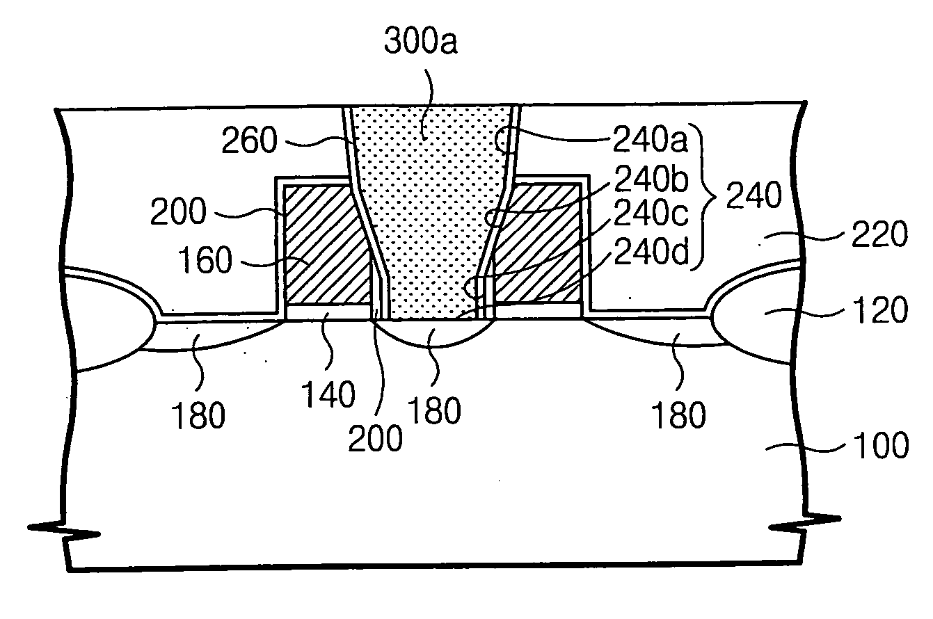
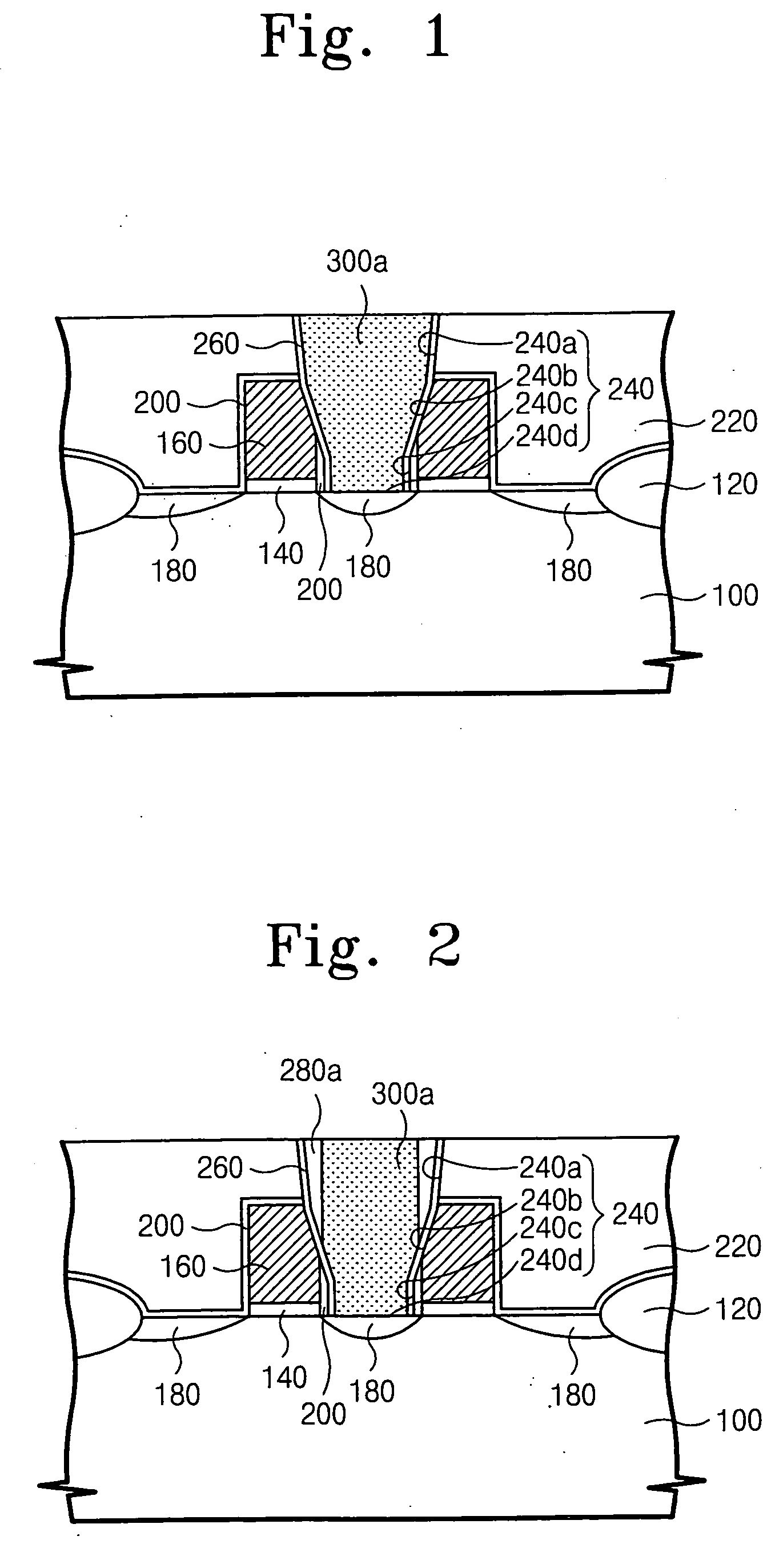
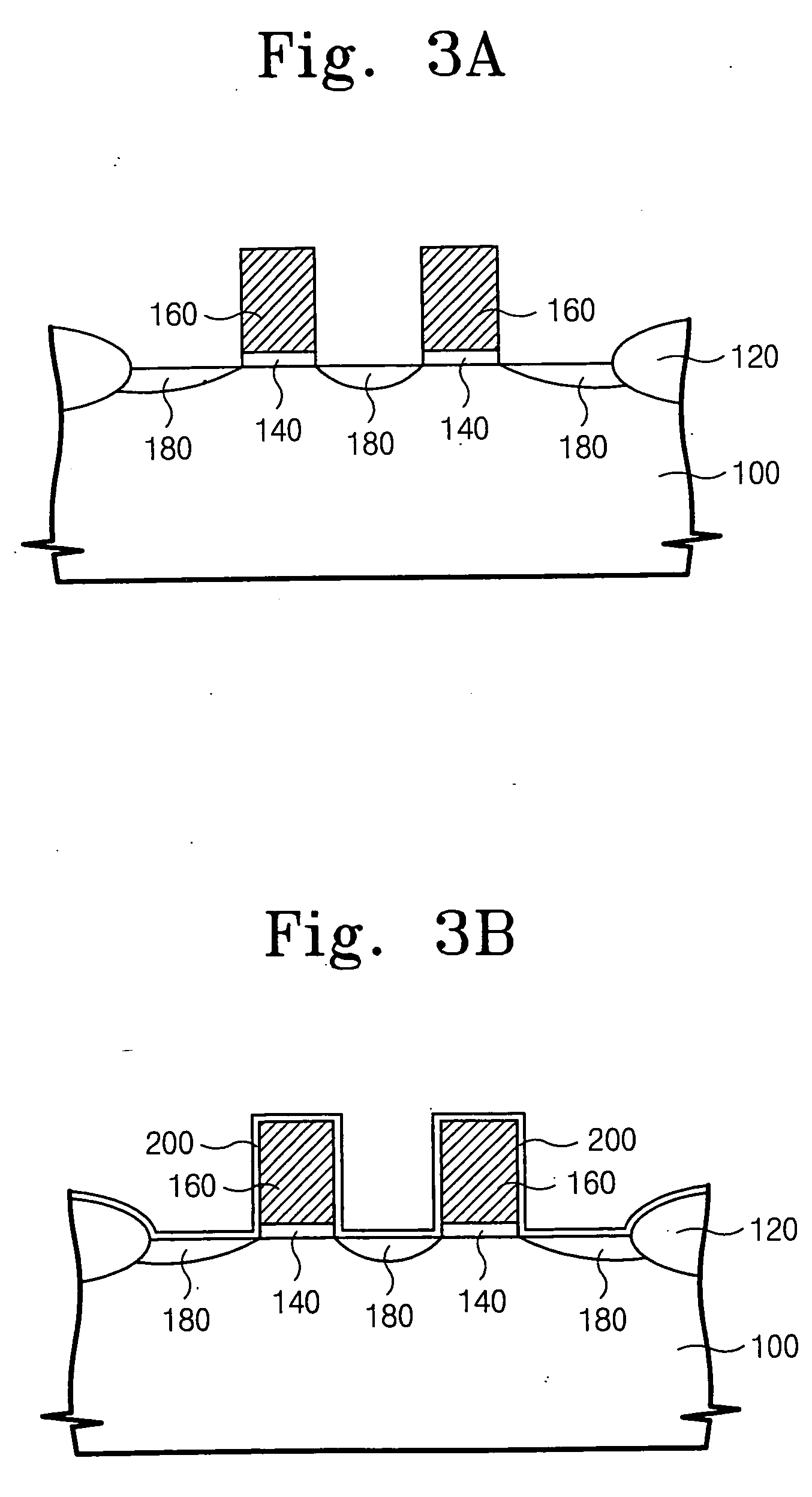
[0051] The present invention will now be described more fully hereinafter with reference to the accompanying drawings, in which embodiments of the invention are shown. Like numbers refer to like elements and repeated explanation of identical elements may be avoided with reference to subsequent figures in the specification. In the figures, certain features, layers or components may be exaggerated for clarity. When a layer is referred to as being “on” another layer or substrate, it can be directly on the other layer or substrate, or intervening layers, films, coatings and the like may also be present unless the word “directly” is used which indicates that the feature or layer directly contacts the feature or layer. In addition, spatially relative terms, such as “beneath”, “below”, “lower”, “above”, “upper” and the like, may be used herein for ease of description to describe one element or feature's relationship to another element(s) or feature(s) as illustrated in the figures. It will...


PUM


Abstract

A self-aligned contact structure and a method of forming the same include selected neighboring gate electrodes with adjacent sidewalls that are configured to angle toward each other. The angled surfaces of the gate electrodes can be protected using a liner layer that can extend the length of the contact window to define the sidewalls of the contact window.

Description

RELATED APPLICATIONS [0001] This application is a continuation of U.S. patent Ser. No. 10 / 695,061, filed Oct. 28, 2003 which claims the benefit of priority to Korean Patent Application 2002-66874, filed on Oct. 31, 2002, the contents of which are incorporated by reference herein in their entirety.FIELD OF THE INVENTION [0002] The present invention relates to semiconductor devices and methods of forming the same and more specifically to lower electrode contact structures over an underlying layer and methods of forming the same. BACKGROUND OF THE INVENTION [0003] Semiconductor device manufacturing typically includes alternately forming conductive layers (or conductive regions) and insulation layers, and electrically connecting upper and lower conductive layers that are otherwise electrically insulated by the insulation layers, using contacts that are formed in predetermined regions of the insulation layer. [0004] For example, when manufacturing a semiconductor memory device, conductiv...

Claims


Application Information

Patent Timeline
Patent Type & Authority Applications(United States)
IPC IPC(8): H01L29/76H01L21/28H01L21/336H01L21/60H01L21/768H01L21/8234H01L21/8242H01L27/088H01L27/10H01L27/108H01L29/423H01L29/49H01L29/78
CPCH01L21/28114H01L21/76831H01L21/76897H01L21/823425H01L21/823475H01L27/10888H01L27/10894H01L29/42376H01L2924/0002H01L2924/00H10B12/485H10B12/09H01L21/28
Inventor KIM, SEONG-HOPARK, DONG-GUNLEE, CHANG-SUBCHOE, JEONG-DONGKIM, SUNG-MINLEE, SHIN-AE
Owner SAMSUNG ELECTRONICS CO LTD
Why Eureka
Try Eureka