Thin film solar cell and manufacturing method thereof

a solar cell and film technology, applied in the direction of pv power plants, light radiation electric generators, generators/motors, etc., can solve the problems of reducing the overall conversion efficiency, reducing production yield, and difficult to form the second opening trench, etc., to suppress the degradation of conversion efficiency and high production yield

Inactive Publication Date: 2006-09-07
SHARP KK
View PDF1 Cites 137 Cited by
  • Summary
  • Abstract
  • Description
  • Claims
  • Application Information

AI Technical Summary

Benefits of technology

[0021] Thus, by the present invention, a thin film solar cell realizing high production yield and suppressing degradation in conversion effi

Problems solved by technology

Therefore, the thin film solar cell shown in FIGS. 6 and 7, which has a plurality of solar cells connected in series by the transparent conductive layer, has a problem that the overall conversion efficiency lowers significantly.
Adjustment of the output of YAG fundamental wave laser beam, however, is difficult, and therefore, process condition is very severe, resulting in a problem of lower production yield.
Specifically, the co

Method used


Image

  • Thin film solar cell and manufacturing method thereof
  • Thin film solar cell and manufacturing method thereof
  • Thin film solar cell and manufacturing method thereof

Examples


example 1

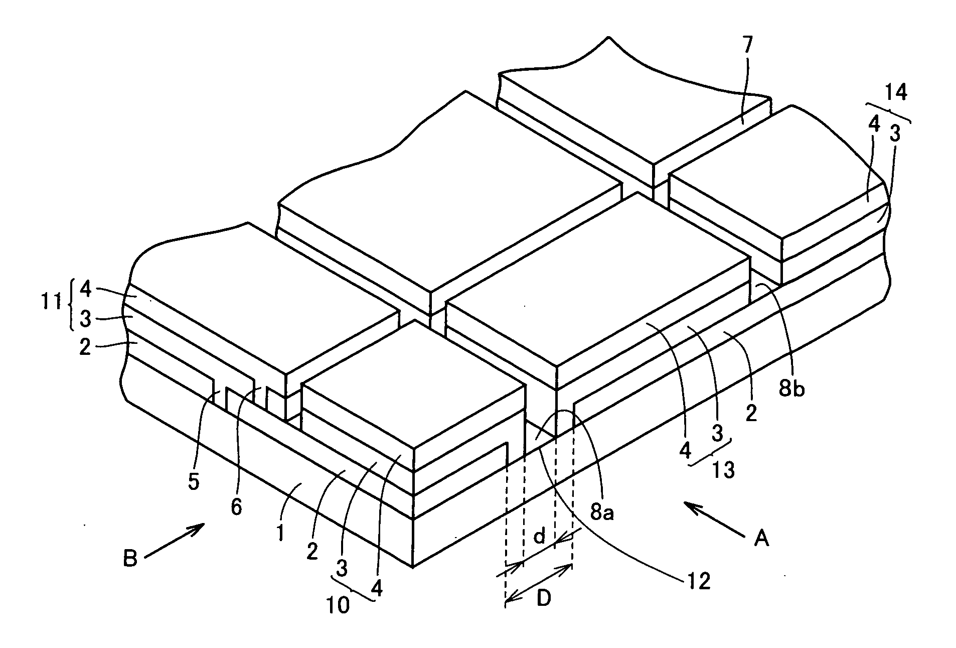
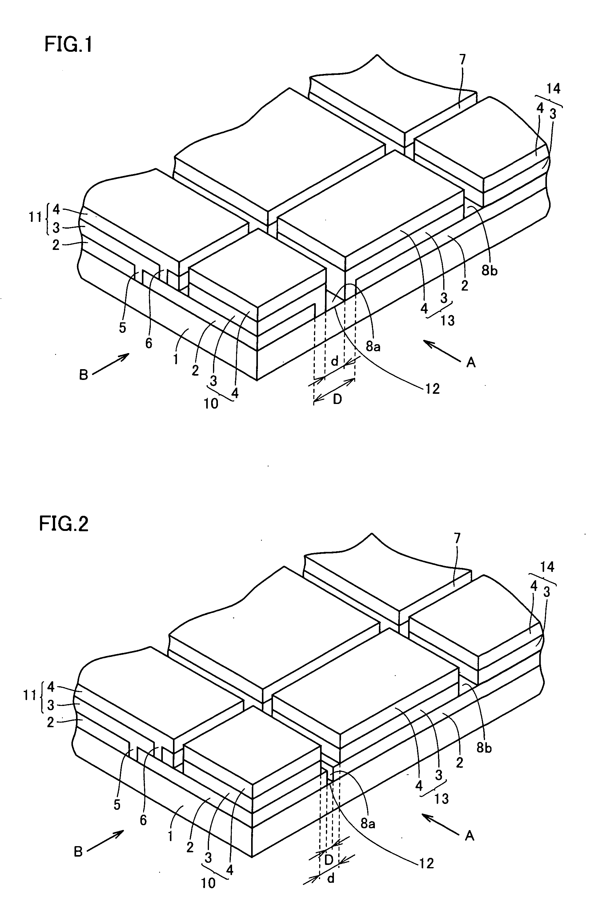
[0048] A glass substrate (Asahi Glass, type U) with a transparent conductive film of SnO2, having the size of 560 mm (width)×925 mm (length) was prepared, and by irradiation of YAG fundamental wave laser beam from the side of the glass substrate, a part of the transparent conductive film was removed in a strip in the width direction of the glass substrate by laser scribing, whereby the second separation trench was formed. The second separation trench had the width of 300 μm, and five second separation trenches were formed at a pitch of 150 mm. Further, in the direction orthogonal to the direction of formation of the second separation trenches (along the length of the glass substrate), by irradiation of YAG fundamental wave laser beam, a part of the transparent conductive film was removed in a strip by laser scribing, and the first separation trench separating the transparent conductive film was formed. The width of the first separation trench was 100 μm, and three first separation t...

example 2

[0054] A glass substrate (Asahi Glass, type U) with a transparent conductive film of SnO2, having the size of 560 mm (width)×925 mm (length) was prepared, and by irradiation of YAG fundamental wave laser beam from the side of the glass substrate, a part of the transparent conductive film was removed in a strip shape in the length direction of the glass substrate by laser scribing, whereby the first separation trench was formed. The first separation trench had the width of 80 μm, and four first separation trenches were formed at a pitch of 150 mm.

[0055] Thereafter, on the transparent conductive film and on the first separation trenches, a photoelectric conversion layer was formed. The photoelectric conversion layer had a tandem structure including p-layer, i-layer and n-layer of amorphous silicon and p-layer, i-layer and n-layer of micro-crystal silicon stacked successively from the side of the glass substrate. Here, the p-layer, i-layer and n-layer of amorphous silicon and p-layer,...


PUM


Abstract

A thin film solar cell includes: a transparent conductive film arranged on a translucent insulating substrate; first and second separation trenches orthogonal to each other on the translucent insulating substrate and separating the transparent conductive film; and a first opening trench parallel to the first separation trench and second opening trenches parallel to said second separation trench, orthogonal to each other on the translucent insulating substrate; wherein solar cells formed on the translucent insulating substrate are arranged at adjacent positions with said first opening trench positioned therebetween and at adjacent positions with said second opening trench positioned therebetween; pairs of said solar cells adjacent to each other with said first opening trench positioned therebetween are electrically connected, and among pairs of solar cells positioned adjacent to each other with the second opening trench in between, some are electrically connected to each other, and others are electrically insulated from each other. Method of manufacturing the thin film solar cell is also provided.

Description

[0001] This nonprovisional application is based on Japanese Patent Application No. 2005-062816 filed with the Japan Patent Office on Mar. 7, 2005, the entire contents of which are hereby incorporated by reference. BACKGROUND OF THE INVENTION [0002] 1. Field of the Invention [0003] The present invention relates to a thin film solar cell and a method of manufacturing the same. Particularly, the present invention relates to a thin film solar cell realizing high production yield and suppressing degradation in conversion efficiency even when a short-circuit occurs in a photoelectric conversion layer, as well as to a method of manufacturing the same. [0004] 2. Description of the Background Art [0005]FIG. 7 is a schematic perspective cross-sectional view showing a part of a conventional thin film solar cell. In the thin film solar cell, on a translucent insulating substrate 1 such as a glass substrate, a strip-shaped transparent conductive film 2 is formed, and on transparent conductive fi...

Claims


Application Information

Patent Timeline
IPC IPC(8): H02N6/00
CPCH01L31/046Y02E10/50H01L31/0468H01L31/0463
Inventor FUJIOKA, YASUSHITAKEDA, TOHRU
Owner SHARP KK
Why Eureka
Try Eureka