Power semiconductor package

a technology of power semiconductor and package, applied in the direction of semiconductor devices, semiconductor/solid-state device details, electrical apparatus, etc., can solve the problems of not being able to achieve the future, not being able to meet the future requirements, and reducing the current density through the connection. , the effect of reducing the current density

Inactive Publication Date: 2006-09-14
INTERNATIONAL RECTIFIER COEP
View PDF16 Cites 11 Cited by
  • Summary
  • Abstract
  • Description
  • Claims
  • Application Information

AI Technical Summary

Benefits of technology

[0007] According to an aspect of the present invention, the fingers allow for connection to the electrodes of the power semiconductor device while the external connection surface of each lead pad, for example, allows for an enlarged area for external connection to a respective conductive pad of a circuit board. The enlarged connection area allows for easier assembly of the package while reducing the current density through the connection between the package and the conductive pad.
[0008] A lead frame in a package according to the present invention may further include at least one more lead for connection to the control electrode of the semiconductor device, or two leads each for connection to a respective control electrode (e.g. when the device is bidirectional), or one to serve as a lead connection to a control electrode and the other to serve as a current sense lead. In the preferred embodiment of the present invention, the connection surfaces of all the leads may be coplanar for easier assembly on a substrate.

Problems solved by technology

Packaging, however, can consume a relatively large area on a circuit board.
While this concept currently contributes to the reduction of the size of a semiconductor package, it may not be a feasible concept in the future.
The reduction in the dimension of the electrodes combined with the improvement in the current carrying density of the semiconductor devices may lead to undesirable results such as premature damage to the conductive adhesive due to the enlarged current density passing through the connection point, high resistance due to the reduced connection cross-section, and difficulty in assembling the die through direct connection of the electrodes to a conductive pad on a circuit board due again to the reduced size of the electrode.

Method used


Image

  • Power semiconductor package
  • Power semiconductor package
  • Power semiconductor package

Examples


first embodiment

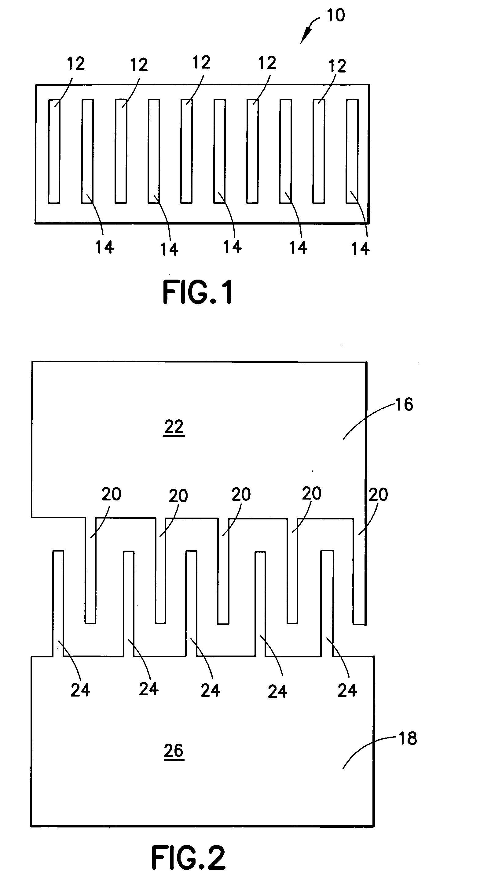
[0029] Semiconductor die 10 in a package may be a schottky device, such as a heterojunction variety III-nitride schottky device based on the InAlGan system, for example, a GaN-based device. A package according to the present invention is not limited to a schottky device, however.

second embodiment

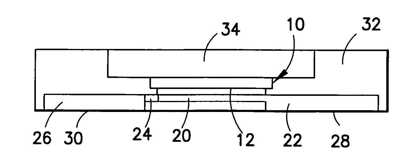
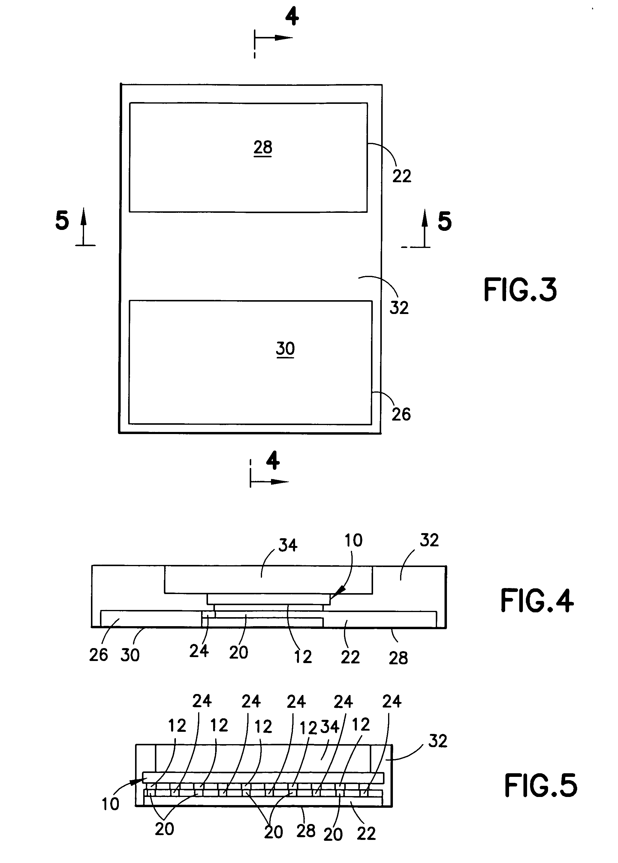
[0030] Referring for example to FIG. 6, in the present invention, semiconductor die 36 may include more electrodes in addition to first and second power electrodes 12, 14. For example, semiconductor die 36 may include two more electrodes 38, 40. In one embodiment, electrodes 38, 40 may each be a control electrode. Such a device may be, for example, a bidirectional device. In another embodiment, electrode 38 may be a control electrode and electrode 40 may be a current sense electrode. In either case, the lead frame may further include a lead 42 that is electrically connected to electrode 36 and another lead 44 that is electrically connected to electrode 40. Once die 36 is assembled onto the lead frame (see FIG. 7), the assembly is overmolded with mold compound. Thus, as seen in FIG. 8, connection surfaces 28, 30 of lead pads 22, 24 are exposed as well as connection surfaces 46, 48 of leads 42, 44. Note that preferably all connection surfaces 46, 48 are coplanar.

[0031] Die 36 in a pac...


PUM


Abstract

A semiconductor package that includes a semiconductor device and a lead frame having a first lead frame portion and a second lead frame portion, each lead frame portion including a plurality of fingers and a lead pad, each finger being electrically connected to a respective electrode of the semiconductor device.

Description

RELATED APPLICATION [0001] This application is based on and claims benefit of U.S. Provisional Application No. 60 / 660,399, filed on Mar. 10, 2005, entitled PACKAGING STRUCTURE FOR GALLIUM NITRIDE DEVICES, to which a claim of priority is hereby made and the disclosure of which is incorporated by reference.BACKGROUND OF THE INVENTION [0002] The present invention relates to semiconductor packages. [0003] It is well known that to incorporate a semiconductor device within a circuit, such a power supply or power regulation circuit, the semiconductor device must be packaged. Packaging, however, can consume a relatively large area on a circuit board. Thus, chip-scale type of packaging has been developed in order to reduce the area that is consumed by a package. [0004] In one variety of chip-scale package, a power electrode of the semiconductor device is readied for direct connection by a conductive adhesive to a conductive pad on a circuit board. While this concept currently contributes to ...

Claims


Application Information

Patent Timeline
Patent Type & Authority Applications(United States)
IPC IPC(8): H01L23/48
CPCH01L23/4334H01L23/4824H01L23/49562H01L2924/0002H01L2924/00H01L23/48
Inventor SCHAFFER, CHRISTOPHER P.
Owner INTERNATIONAL RECTIFIER COEP
Why Eureka
Try Eureka