Current balancing circuit
- Summary
- Abstract
- Description
- Claims
- Application Information
AI Technical Summary
Benefits of technology
Problems solved by technology
Method used
Image

Examples
first embodiment
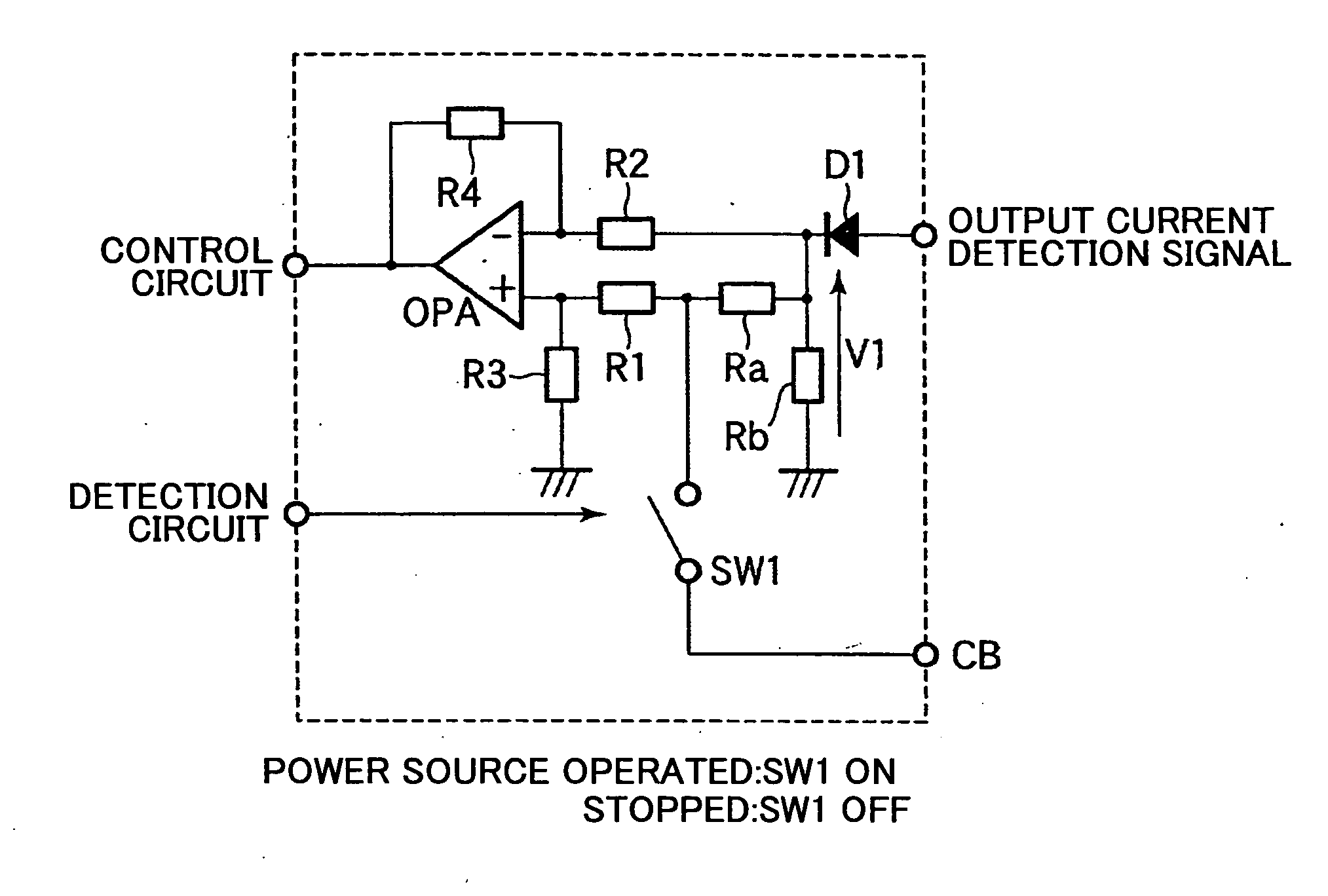
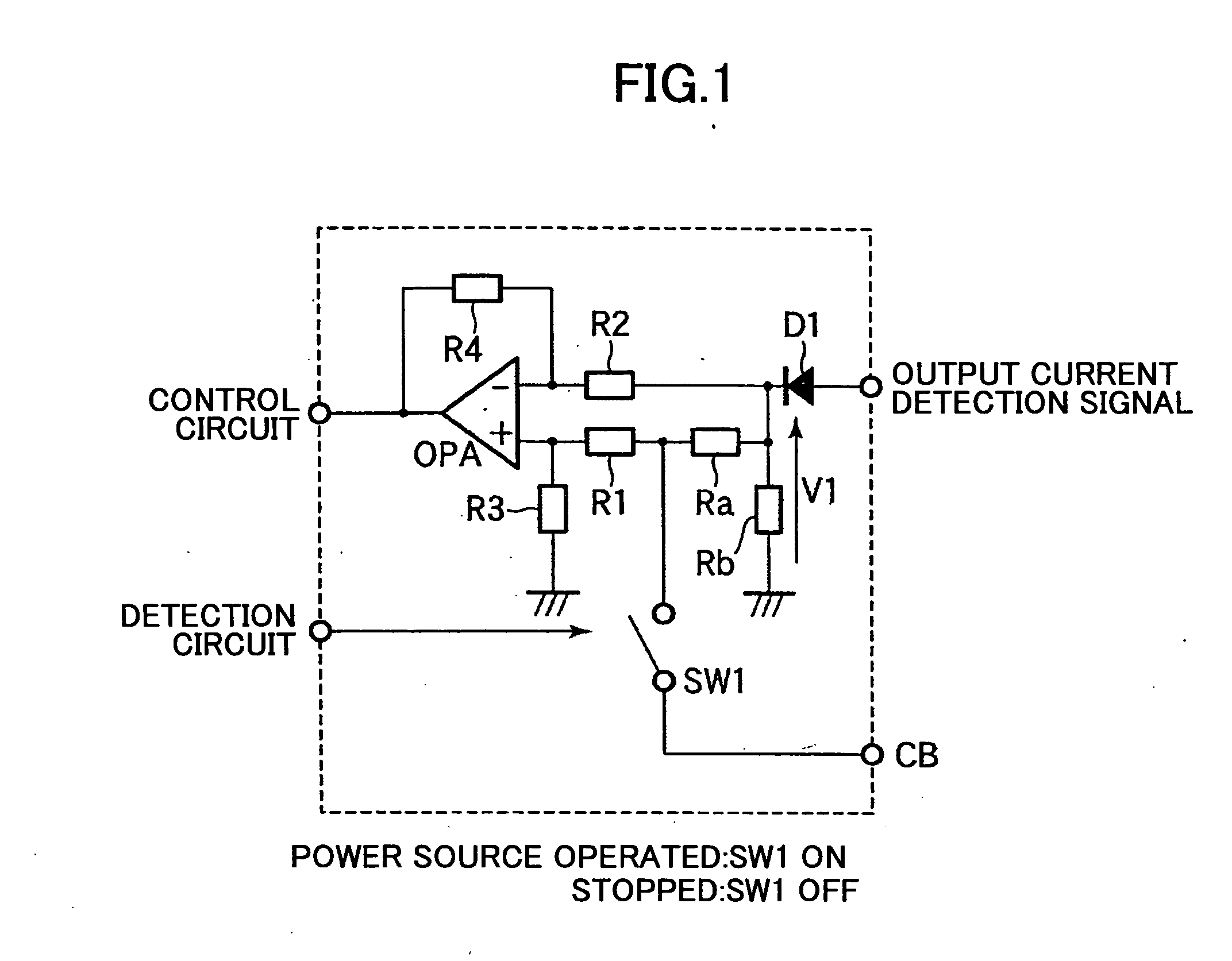
[0029]FIG. 1 is a circuit diagram illustrating a current balancing circuit according to a first embodiment of the present invention. The current balancing circuit comprises an operational amplifier OPA, resistors R1-R4, first and second resistors Ra and Rb, a diode D1, a switching circuit SW1, and a current balancing terminal CB. The first resistor Rb receives an output current detection signal input via the diode D1 and outputs the signal as an output current detection voltage v1. The second resistor Ra is connected between the current balancing terminal CB and a connection point between the first resistor Rb and the diode D1. The operational amplifier OPA receives an output current detection voltage, which is applied to the current balancing terminal CB from another current balancing circuit, via a connection point between the second resistor Ra and the current balancing terminal CB and the input resistor R1, and receives the output current detection voltage V1 via a connection po...
second embodiment
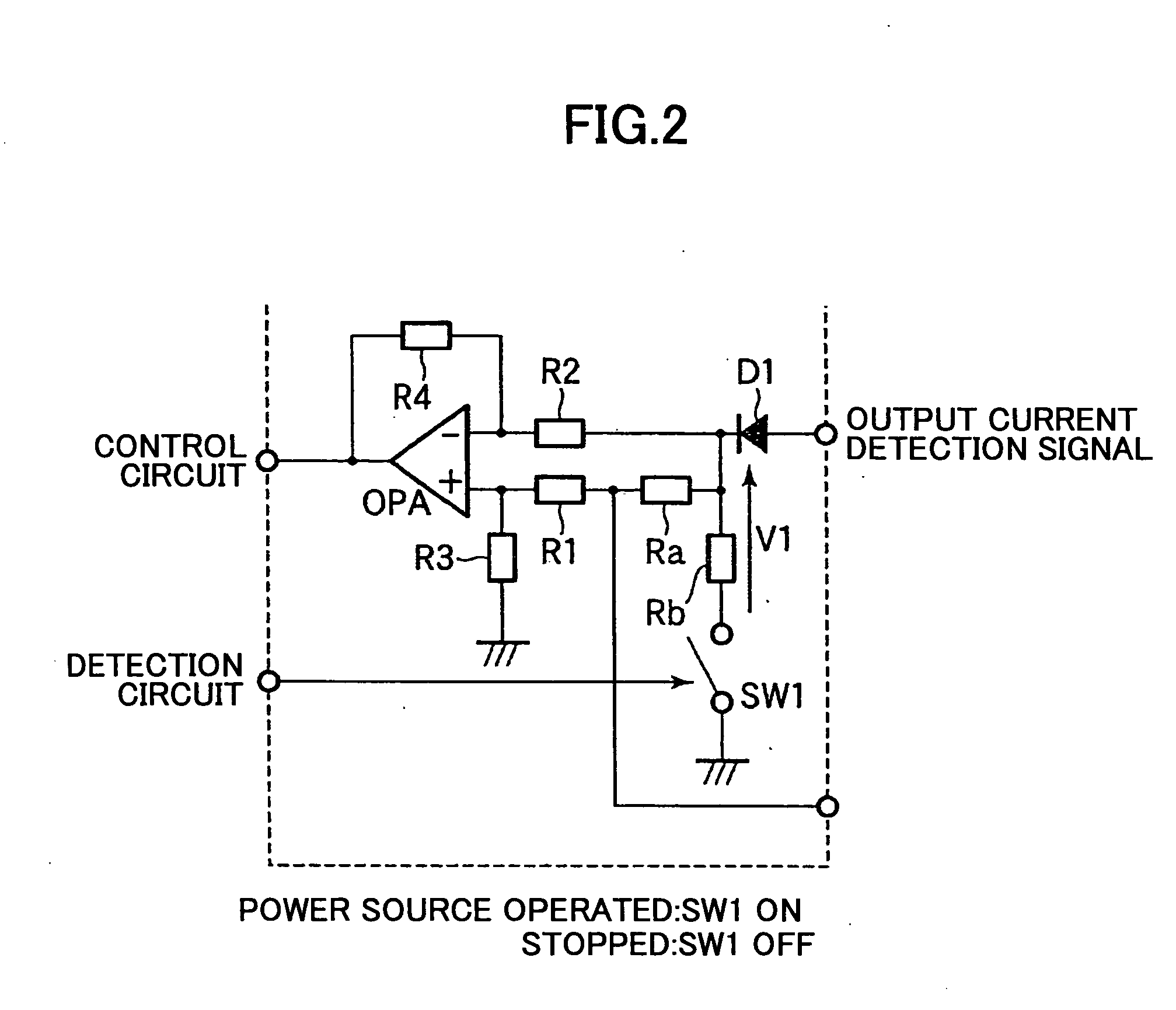
[0032]FIG. 2 is a circuit diagram illustrating a current balancing circuit according to a second embodiment of the present invention, wherein elements identical to those in FIG. 1 bear the same reference numbers. In the second embodiment, a switching circuit SW1 connects and disconnects a first resistor Rb to and from ground. The switching circuit is turned off in response to detection of a power failure, and is turned on when the power source operates normally. As in the first embodiment, while the power source operates normally, the switching circuit SW1 remains on so as to control the current balance. When a detection circuit detects a power failure, the switching circuit SW1 is turned off so as to disconnect the second and first resistors Ra and Rb from ground, thereby preventing lowering of the impedance of a current balance control system. Although a current balancing terminal CB is grounded via resistors R1 and R3, that has little effect on the lowering of the impedance of th...
third embodiment
[0033]FIG. 3 is a block diagram illustrating a switching power supply unit according to a third embodiment of the present invention. The power supply unit comprises a transformer 1, a rectifier circuit 2, a smoothing circuit 3, an output voltage detection circuit 4, an output current detection circuit 5, a current balancing circuit 6, a control circuit 7, a determination circuit 10, an input voltage monitoring part 11, an input current monitoring part 12, a circuit failure monitoring part 13, a temperature monitoring part 14, a switching transistor Q1, and a current balancing terminal CB. Vin and Vout indicate an input voltage and an output voltage, respectively. The current balancing circuit 6 may have the configuration shown in FIG. 1 or the configuration shown in FIG. 2.
[0034] The input voltage Vin is applied to the transformer 1. The control circuit 7 controls switching operations of the switching transistor Q1 connected to a primary winding of the transformer 1. An induced vol...
PUM
 Abstract
Description
Claims
Application Information
 - Generate Ideas
- Intellectual Property
- Life Sciences
- Materials
- Tech Scout
- Unparalleled Data Quality
- Higher Quality Content
- 60% Fewer Hallucinations
Browse by: Latest US Patents, China's latest patents, Technical Efficacy Thesaurus, Application Domain, Technology Topic, Popular Technical Reports.
© 2025 PatSnap. All rights reserved.Legal|Privacy policy|Modern Slavery Act Transparency Statement|Sitemap|About US| Contact US: help@patsnap.com