Method of fabricating flash memory device

a flash memory and memory device technology, applied in the direction of semiconductor devices, basic electric elements, electrical appliances, etc., can solve the problems of data loss, data loss in the dram, and inability to maintain data when not being powered,

Active Publication Date: 2006-09-14
SK HYNIX INC
View PDF2 Cites 4 Cited by
  • Summary
  • Abstract
  • Description
  • Claims
  • Application Information

AI Technical Summary

Benefits of technology

[0015] Accordingly, the present patent addresses the above problems, and it is an object of the present patent to disclose a method of fabricating a flash memory device, wherein the capacitance of an interlayer dielectric film can be secured without loss, while preventing a stringer of a control gate from being formed.
[0016] The patent also discloses a method of fabricating a flash memory device, in which the program speed can be enhanced.
[0027] When removing the element isolation films in the step (f), the process can be controlled so that the surface of the element isolation films does not becomes lower than the floating gates.

Problems solved by technology

The volatile memory has characteristics in which it can maintain data when being powered, but cannot maintain data when not being powered.
If not being powered, data within the DRAM is automatically lost.
In SRAM, data are also automatically lost if not being powered.
Upon etching of the stack gate, however, a stringer is inevitably formed in which neighboring control gates are connected because the control gates remain due to a shadowing effect by the floating gate having the negative slope.
Therefore, there is a problem in that the coupling ratio is lowered.
In this case, the ability in which a voltage applied to the control gate is transferred to the floating gate is lowered, resulting in a reduction in the program speed.

Method used


Image

  • Method of fabricating flash memory device
  • Method of fabricating flash memory device
  • Method of fabricating flash memory device

Examples


Embodiment Construction

[0040] Various embodiments will be described with reference to the accompanying drawings. Those of ordinary skill in the art will appreciate that the disclosed embodiments may be modified in various manners and the scope of the present patent is not limited by the embodiments described later.

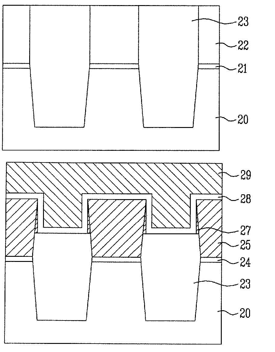
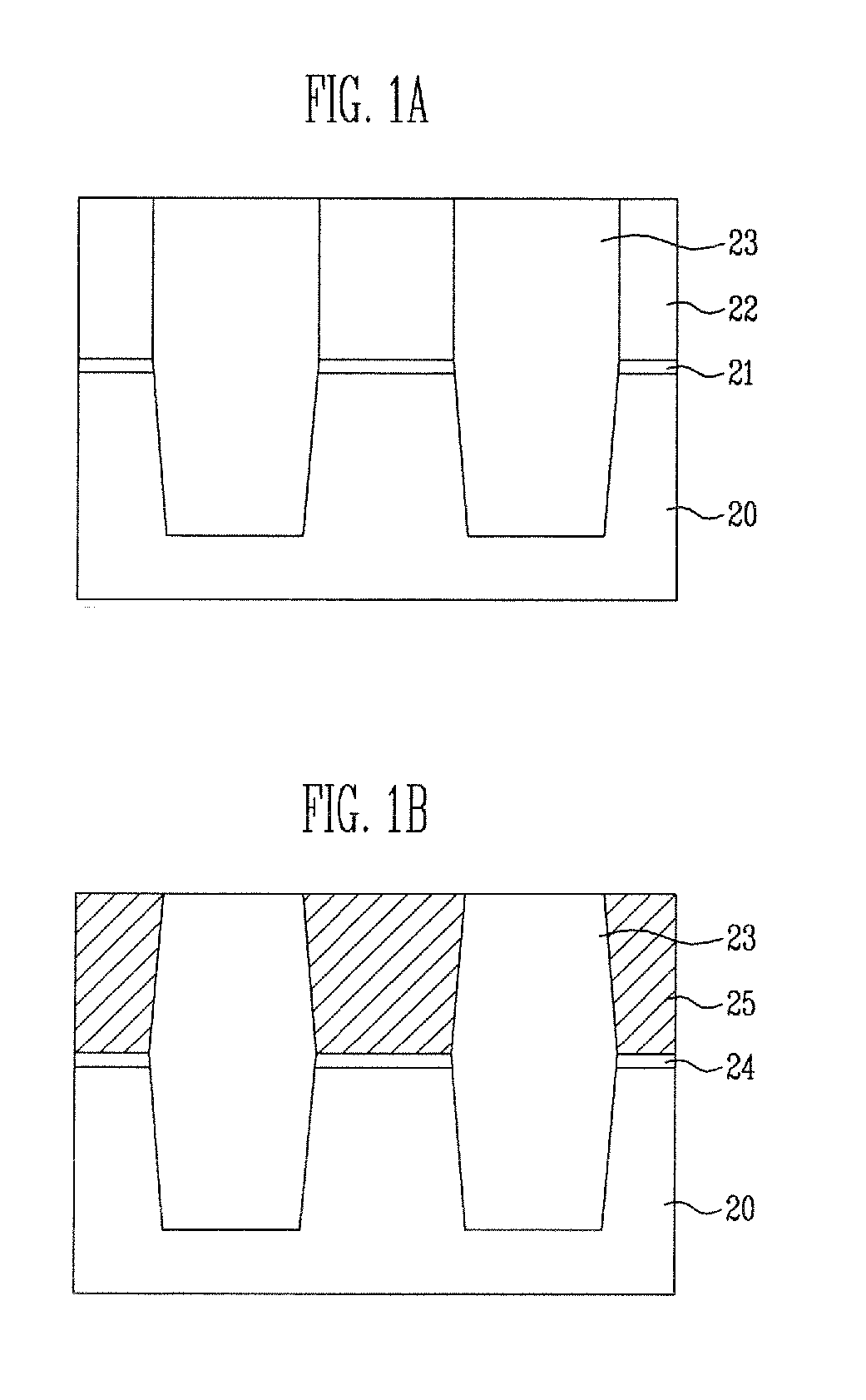
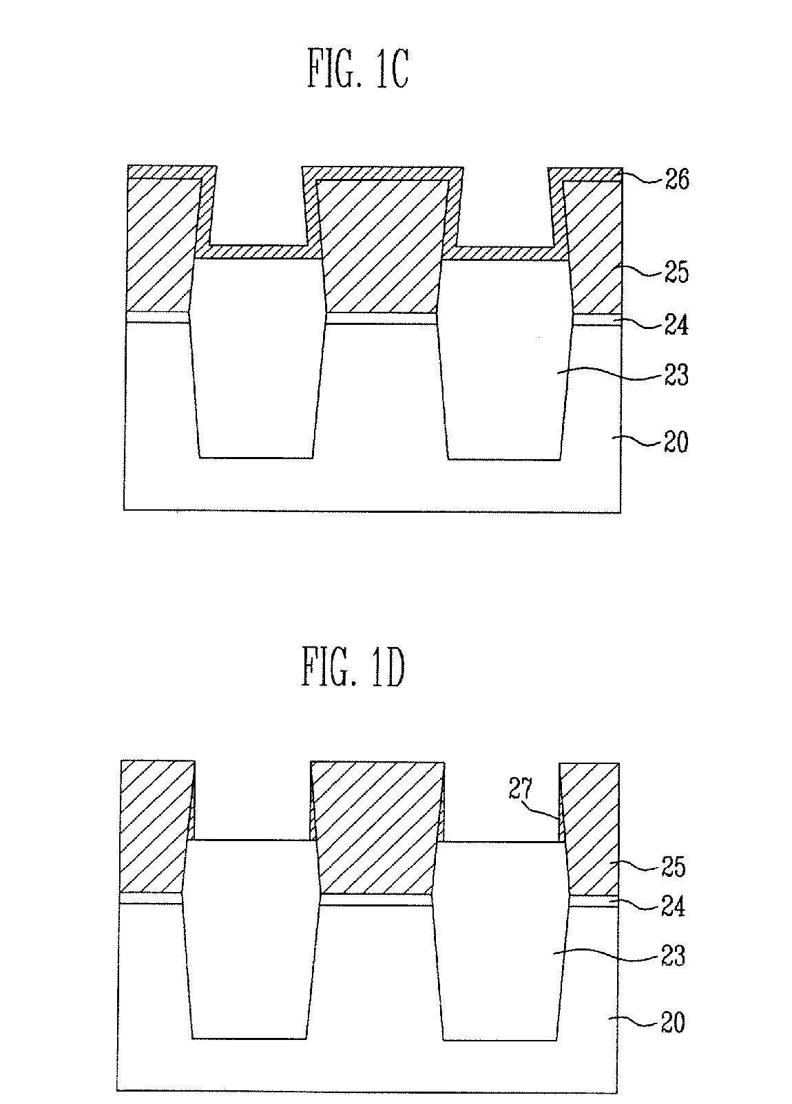
[0041]FIGS. 1a to 1e are cross-sectional view illustrating process steps in an exemplary method of fabricating a flash memory device.

[0042] In the method of fabricating the flash memory device according to the disclosed embodiment of the present patent, a pad insulating film 21 and a hard mask film 22 are first sequentially formed on a semiconductor substrate 20, as shown in FIG. 1a.

[0043] The pad insulating film 21 can be formed to a thickness of 20 to 200 {acute over (Å)} using an oxide film, and the hard mask film 22 can be formed to a thickness of 300 to 3000 {acute over (Å)} using a silicon nitride film.

[0044] The hard mask film 22 and the pad insulating film 21 are selectively removed ...


PUM


Abstract

A method of fabricating a flash memory device is disclosed wherein, electrode spacers are formed on sides of self-aligned floating gates having a negative slope. Thus, upon etching of a stack gate after an interlayer dielectric film and a control gate are formed, a stringer of a control gate, which is formed by the negative slope of the self-aligned floating gates, can be prevented. Furthermore, because an isotropic etch process is used to remove element isolation films between the floating gates, the element isolation films do not remain on the sides of the floating gates. It is thus possible to prevent loss of the coupling ratio. Accordingly, failure of devices can be reduced and decreasing the program speed can be prevented.

Description

CROSS REFERENCE TO RELATED APPLICATIONS [0001] This application relies for priority upon Korean Patent Application No. 2005-20238 filed on Mar. 10, 2005, the contents of which are herein incorporated by reference in their entirety. FIELD OF THE INVENTION [0002] The present patent relates to a method of fabricating a flash memory device, and more specifically, to a method of fabricating a flash memory device, wherein the capacitance of an interlayer dielectric film can be secured without loss while preventing formation of a stringer of a control gate. DISCUSSION OF RELATED ART [0003] Generally, semiconductor memory devices are largely classified into a volatile memory and a non-volatile memory. [0004] Volatile memory includes RAMs such as DRAM (Dynamic Random Access Memory) and SRAM (Static Random Access Memory). The volatile memory has characteristics in which it can maintain data when being powered, but cannot maintain data when not being powered. [0005] In DRAM, transistors have a...

Claims


Application Information

Patent Timeline
Patent Type & Authority Applications(United States)
IPC IPC(8): H01L21/336
CPCH01L27/115H01L27/11521H10B69/00H10B41/30H10B99/00
Inventor LEE, SEOK KIU
Owner SK HYNIX INC
Why Eureka
Try Eureka