Organic electroluminescent device, driving method thereof and electronic apparatus

an electroluminescent device and organic technology, applied in static indicating devices, instruments, transportation and packaging, etc., can solve problems such as complicated signal processing, and achieve the effects of controlling luminance, high contrasted images, and controlling luminan

Inactive Publication Date: 2006-09-21
SEIKO EPSON CORP
View PDF12 Cites 18 Cited by
  • Summary
  • Abstract
  • Description
  • Claims
  • Application Information

AI Technical Summary

Benefits of technology

[0007] An advantage of the present invention is to provide an organic EL device that is capable of controlling luminance in accordance with the ratio of a light-emission area to an entire display without changing a voltage applied in accordance with the ratio, a method for driving the organic EL device, and an electronic apparatus having the organic EL device.
[0008] An organic electroluminescent (EL) device according to one aspect of the invention includes a plurality of pixels each having a light-emitting element, and a drive device adjusting a light-emission period of the light-emitting element included in each pixel in accordance with a luminance ratio of an image to be displayed.
[0009] Since the light-emission period of the light-emitting element included in each pixel is adjusted in accordance with the luminance ratio of an image to be displayed (the ratio of an emission area to an entire display), it is possible to make the emission period long when the luminance ratio is small and make the emission period short when the luminance ratio is large, for example. As a result, luminance can be controlled depending on the luminance ratio of an image to be displayed without changing a voltage applied to the light-emitting element, thereby providing highly contrasted images as the CRT does.
[0010] Here, the luminance ratio of an image to be displayed refers to the ratio of an integrated luminance when every light-emitting element in the viewing area of an organic EL display produces luminescence at a maximum to an integrated luminance when only some light-emitting elements that are required in accordance with the image produce luminescence. Assuming that Lmax represents the maximum luminance of individual light-emitting elements and Lk is the number of light-emitting elements that are required to produce luminescence in accordance with image) represents a luminance of individual light-emitting elements when only required light-emitting elements produce luminescence, the luminance ratio Lr of the image satisfies the formula (1):
[0011] In the organic EL device, the drive device may adjust the light-emission period of the light-emitting element by adjusting non-emission timing of the light-emitting element included in each of the pixels.
[0012] Since the light-emission period of the light-emitting element is adjusted by adjusting non-emission timing of the light-emitting element, it is possible to control luminance in accordance with a luminance ratio of an image to be displayed without making the driving and structure of the light-emitting element much complicated.

Problems solved by technology

For example, to represent ten grayscale levels with an organic EL element to which a voltage of 10 V at a maximum is applied, the voltage applied to the element is varied by 1 V. However, when a voltage of 15 V at a maximum is applied to the organic EL element to provide the peak luminance display, the voltage applied to the element to represent every grayscale level has to be varied by 1.5 V. The method of related art therefore makes signal processing complicated.

Method used


Image

  • Organic electroluminescent device, driving method thereof and electronic apparatus
  • Organic electroluminescent device, driving method thereof and electronic apparatus
  • Organic electroluminescent device, driving method thereof and electronic apparatus

Examples


first embodiment

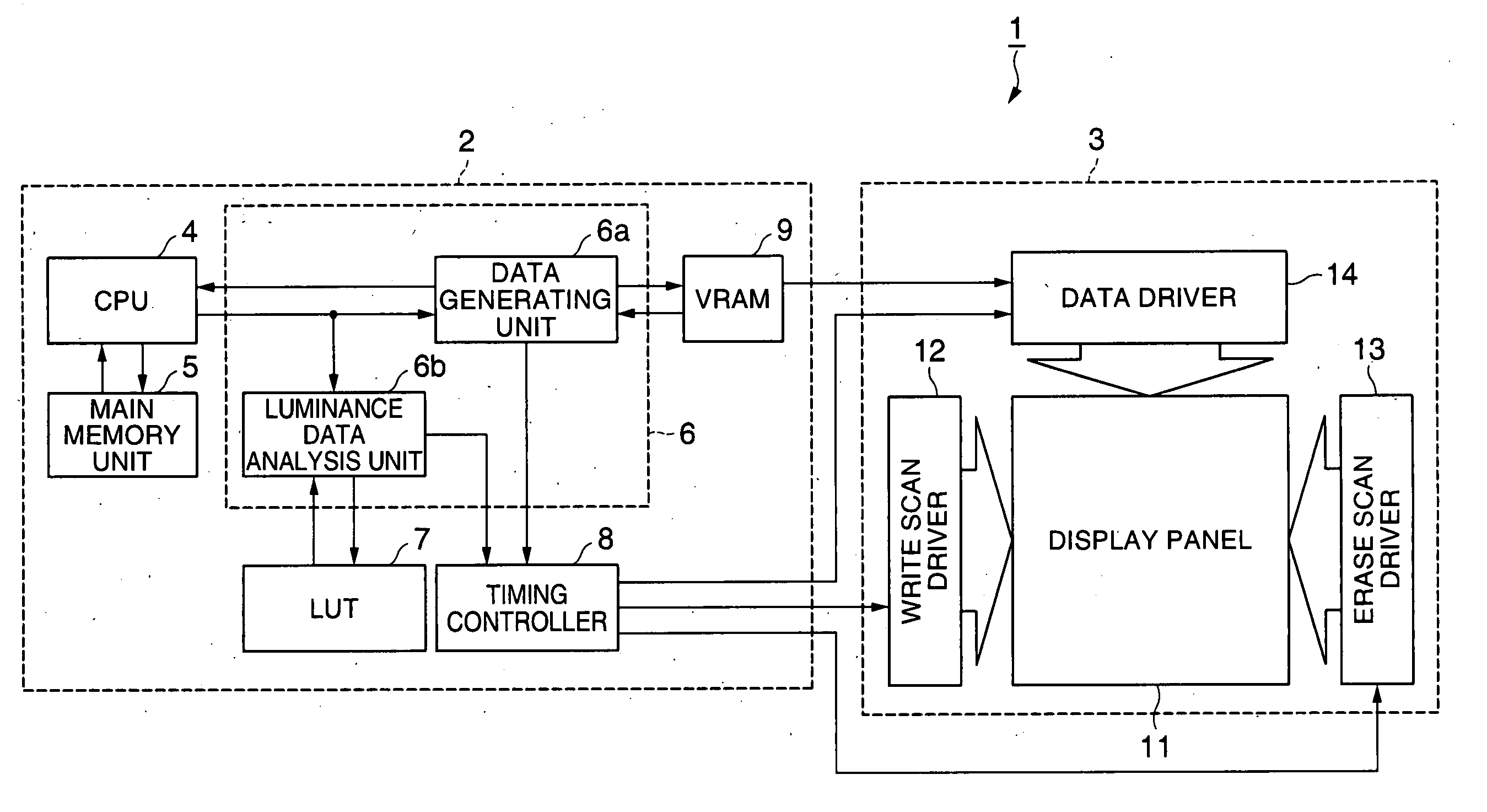
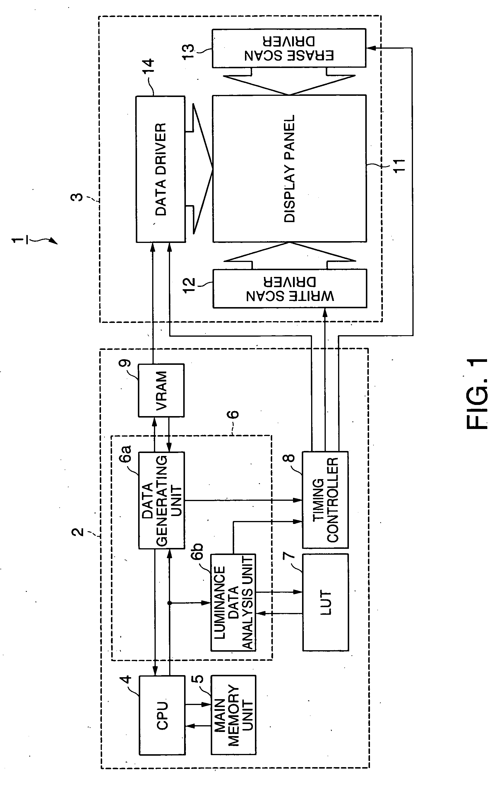
[0058]FIG. 1 is a block diagram illustrating the electrical structure of an organic EL device according to a first embodiment of the invention. Referring to the diagram, this organic EL device 1 includes a peripheral drive device 2 and a display panel unit 3. The peripheral drive device 2 includes a central processing unit (CPU) 4, a main memory unit 5, a graphics controller 6, a lookup table (LUT) 7, a timing controller 8 and a video RAM (VRAM) 9. The CPU 4 may be replaced with a microprocessor unit (MPU). The display panel unit 3 includes a display panel 11, a write scan driver 12, an erase scan driver 13 and a data driver 14.

[0059] The CPU included in the peripheral drive device 2 reads image data stored in the main memory unit 5, carries out various types of processing, such as expansion, with the main memory unit 5, and outputs processed data to the graphics controller 6. The graphics controller 6 produces image data and synchronizing signals (vertical and horizontal synchroni...

second embodiment

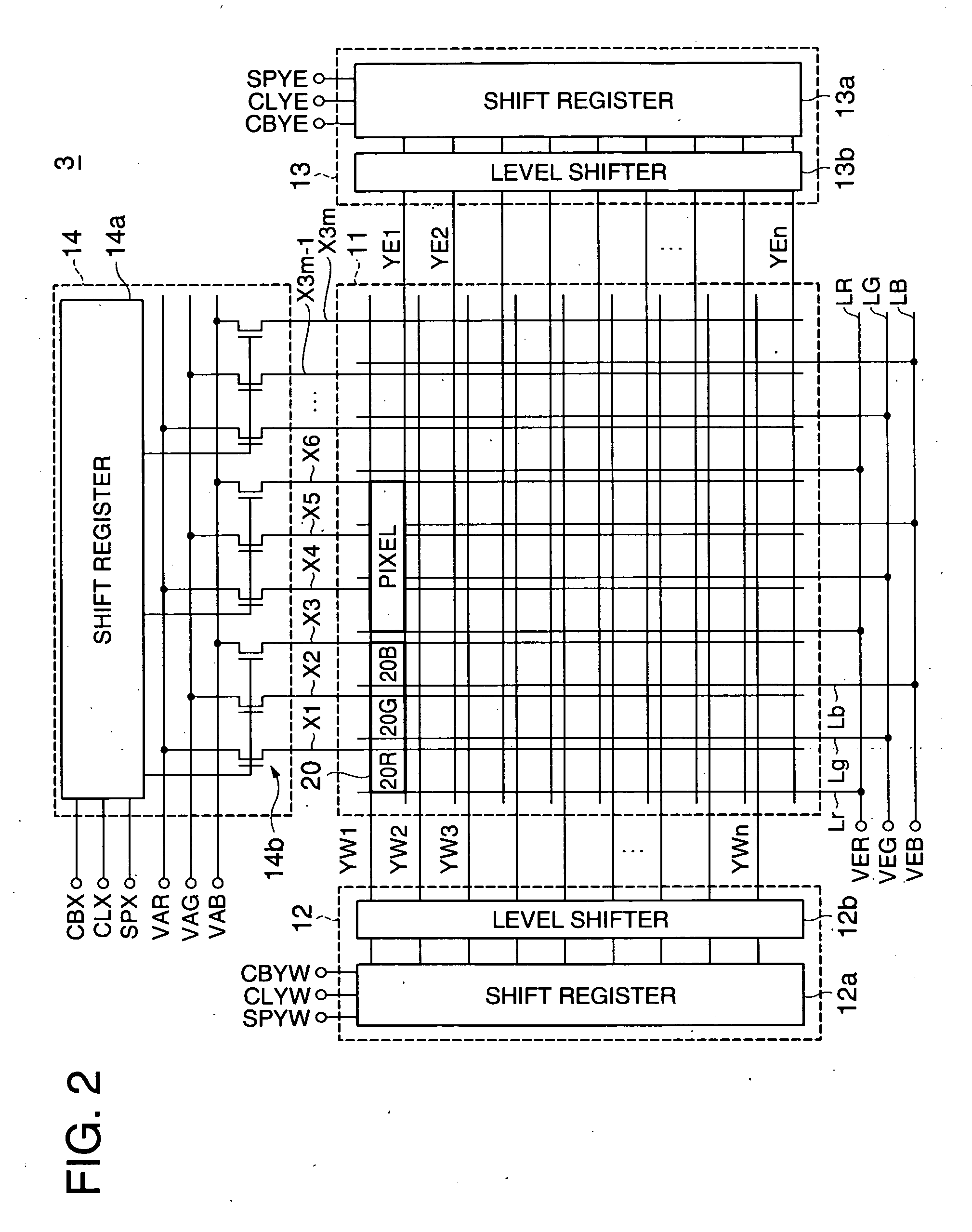
[0115]FIG. 10 is a block diagram illustrating the electrical structure of an organic EL device according to a second embodiment of the invention. The same numerals as given in FIG. 1 indicate the same elements here. Referring to FIG. 10, this organic EL device of the second embodiment has the structure of the first embodiment shown in FIG. 1 as a basis in which the erase scan driver 13 is omitted and the display panel 11, the write scan driver 12 and the data driver 14 are replaced with a display panel 15, a scan driver 16 and a data driver 17. Also, the timing controller 8 shown in FIG. 1 is replaced with a timing controller 8a.

[0116] The timing controller 8 shown in FIG. 1 produces the write scan driver clock signal CLYW and the inverted write scan driver clock signal CBYW and outputs them to the write scan driver 12. The timing controller 8a shown in FIG. 10 instead produces a scan driver clock signal CLY and an inverted scan driver clock signal CBY and outputs them to the scan ...


PUM


Abstract

An organic electroluminescent device, comprises a plurality of pixels each including a light-emitting element, and a drive device adjusting a light-emission period of the light-emitting element included in each of the pixels in accordance with a luminance ratio of an image to be displayed.

Description

BACKGROUND [0001] 1. Technical Field [0002] The present invention relates to an organic electroluminescent (EL) device, a method for driving the organic EL device, and an electronic apparatus. [0003] 2. Related Art [0004] An organic EL device having an organic EL element as a light-emitting element that requires no backlight has been drawing attention recently. This organic EL element is made up of a pair of opposing electrodes and an organic EL layer, i.e. a light-emitting element, provided between the electrodes. The organic EL device that provides a full-color display includes a light-emitting element having a range of emission wavelengths for red, green and blue. As a voltage is applied to between the pair of electrodes, injected electrons and holes recombine in the light-emitting element, thereby the element emits light. The light-emitting element included in this organic EL device is formed of a thin film whose thickness is typically less than 1 micrometer. In addition, the de...

Claims


Application Information

Patent Timeline
Patent Type & Authority Applications(United States)
IPC IPC(8): G09G3/30H05B44/00
CPCG09G3/3233G09G3/3266G09G3/3291G09G2300/0842G09G2310/0251G09G2310/061G09G2360/16B60Q1/143B60Q1/0023B60Q2300/314B60Q2300/054B60Y2200/11
Inventor HARA, HIROYUKI
Owner SEIKO EPSON CORP
Why Eureka
Try Eureka