

Quantum dot white light diode
- Summary
- Abstract
- Description
- Claims
- Application Information
AI Technical Summary
Benefits of technology
Problems solved by technology
Method used
Image

Examples
embodiment one
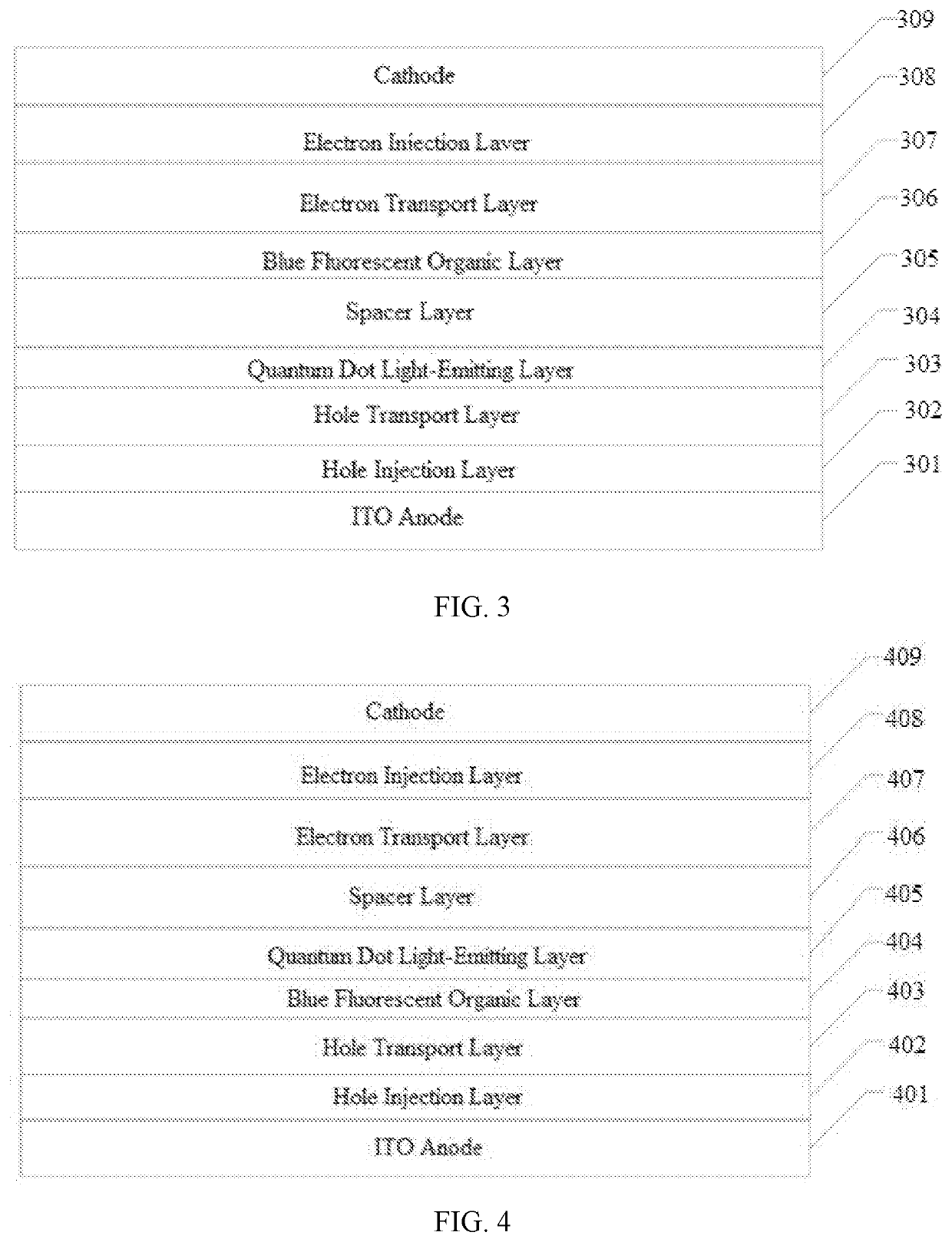
[0100]For example, as shown in FIG. 3, TCTA: TmPyPb mixed material is used as the spacer material. The quantum dot white light-emitting diodes include: an ITO anode 301, a hole injection layer 302, a hole transport layer 303, a quantum dot light-emitting layer 304, a spacer layer 305, a blue fluorescent organic layer 306, an electron transport layer 307, an electron injection layer 308 and a cathode 309. The specific preparation includes the following steps: depositing PEDOT: PSS by solution method on a patterned ITO glass as a hole injection layer having a thickness of 30 nm; depositing TFB by solution method on the PEDOT: PSS as a hole transport layer having a thickness of 30 nm; depositing mixed red and green quantum dots by solution method on the TFB as a quantum dot light-emitting layer having a thickness of 15 nm; depositing TCTA: TmPyPb mixed material by co-evaporation method on the quantum dot light-emitting layer as a spacer layer having a thickness of 8 nm; depositing POTA...
embodiment two
[0101]In an embodiment, CBP is used as the spacer material, quantum dot white light-emitting diodes include: a ITO anode, a hole injection layer, a hole transport layer, a quantum dot light-emitting layer, a spacer layer, a blue fluorescent organic layer, an electron transport layer, an electron injection layer, and a cathode. The specific preparation includes the following steps: depositing PEDOT: PSS by solution method on a patterned ITO glass as a hole injection layer having a thickness of 30 nm; depositing TFB by solution method on the PEDOT: PSS as a hole transport layer having a thickness of 30 nm; depositing the CBP: red and green quantum dot mixed material by solution method on the TFB as the quantum dot light-emitting layer having a thickness of 20 nm; depositing CBP by vapor deposition on the quantum dot light-emitting layer as the spacer layer having a thickness of 8 nm; depositing POTA and CBP by vapor deposition on the spacer layer as a blue fluorescent organic layer ha...
embodiment three
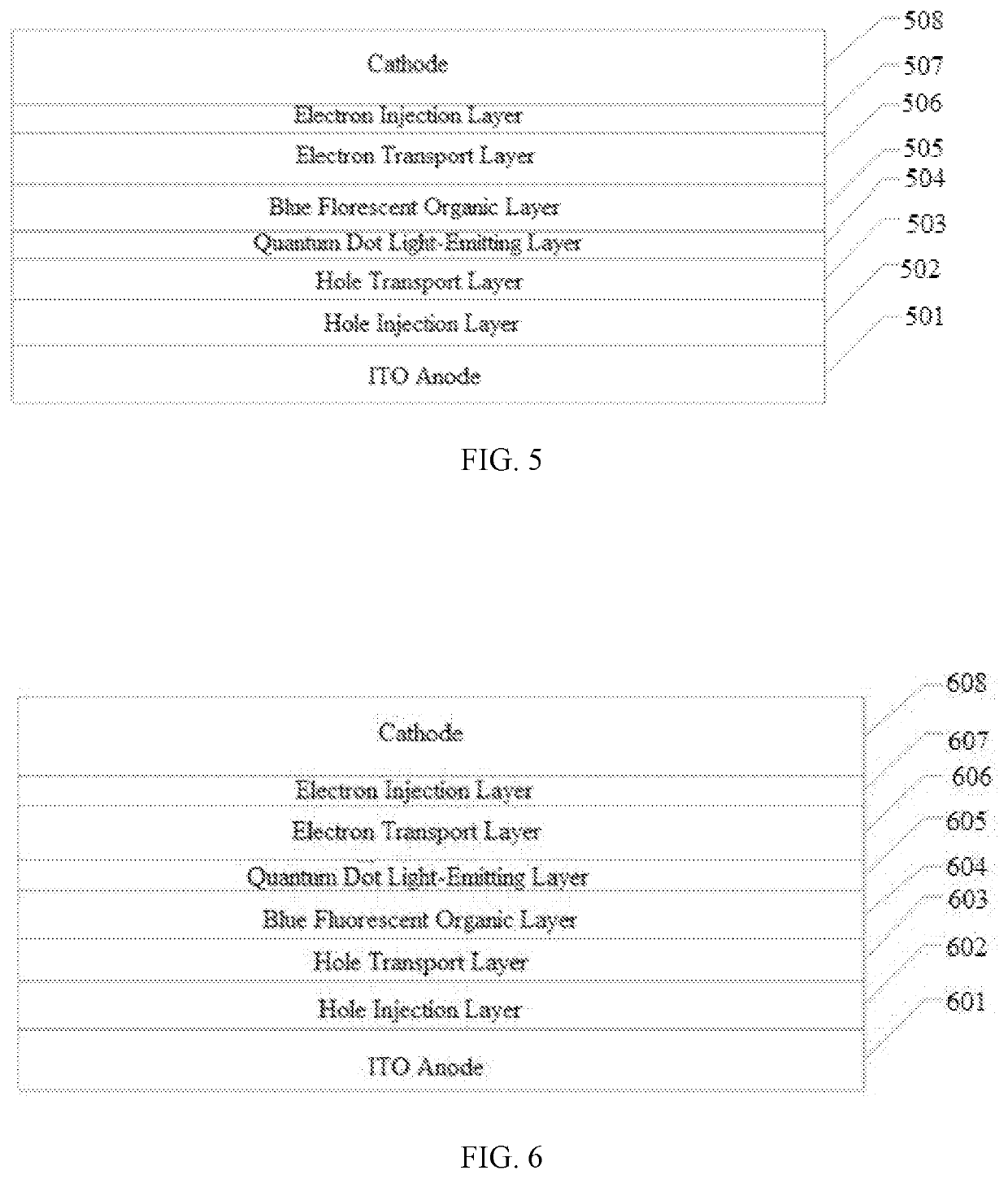
[0102]In an embodiment, TCTA: TPBi mixed material is used as the spacer material. As shown in FIG. 4, the quantum dot white light-emitting-emitting diode include sequentially from bottom to top: a ITO anode 401, a hole injection layer 402, a hole transport layer 403, a blue fluorescent organic layer 404, a quantum dot light-emitting layer 405, a spacer layer 406, an electron transport layer 407, an electron injection layer 408 and a cathode 409. The specific preparation includes the following steps: depositing PEDOT: PSS on a patterned ITO glass as a hole injection layer having a thickness of 30 nm; depositing TFB by solution method on the PEDOT: PSS as a hole transport layer having a thickness of 30 nm; depositing POTA and TCTA: TmPyPb by co-evaporation method on the TFB as a blue fluorescent organic layer having a thickness of 15 nm; depositing sequentially stacked red and green quantum dot films by solution method on the blue fluorescent organic layer as a quantum dot light-emitt...
PUM
 Abstract
Description
Claims
Application Information