Supercharge Your Innovation With Domain-Expert AI Agents!

Electronic devices

a technology of electronic devices and semiconductor materials, applied in the field of electronic devices, can solve the problems of short life of a number of organic electronic devices, degradation and/or doping of semiconductor materials, and not being considered as suitabl

Active Publication Date: 2006-09-28
XEROX CORP
View PDF24 Cites 49 Cited by
  • Summary
  • Abstract
  • Description
  • Claims
  • Application Information

AI Technical Summary

Benefits of technology

The present patent provides electronic devices and thin film transistors (TFTs) with a wax coating that encapsulates the active layer, providing stability and protection from environmental factors such as oxygen and moisture. The wax coating acts as a protective layer and also prevents the adverse effects of oxygen on the device's performance. The wax coating can be deposited on the device using a vacuum deposition method. The use of a wax coating allows for the separation of the device from its environment, providing a more robust and reliable electronic device. The wax coating can also enhance the current on / off ratio of the TFTs and improve their performance.

Problems solved by technology

Unfortunately, the lifetime of a number of organic electronic devices is usually short when the devices are exposed to ambient conditions in view of certain interactions of the organic semiconductor layer with the ambient oxygen, moisture, and light causing degradation and / or doping of the semiconductor materials.
Silicon oxide usually involves vacuum deposition, thus, it is not considered as being suitable with a number of OTFTs (organic thin film transistors) fabricated by solution coating or jet printing processes.
PVA and PVP are hydrophilic and over time absorb moisture from the air and degrade TFT performance.
PMMA is amorphous and may not effectively block environmental oxygen from entering the devices.
Nonetheless, many of the semiconductor polythiophenes are not, it is believed, stable when exposed to air as they become oxidatively doped by ambient oxygen, resulting in increased conductivity.
The result is larger off-current and thus lower current on / off ratio for the devices fabricated from these materials.
These precautionary measures add to the cost of manufacturing therefore offsetting the appeal of certain polymer TFTs as an economical alternative to amorphous silicon technology, particularly for large area devices.

Method used


Image

  • Electronic devices
  • Electronic devices
  • Electronic devices

Examples


Embodiment Construction

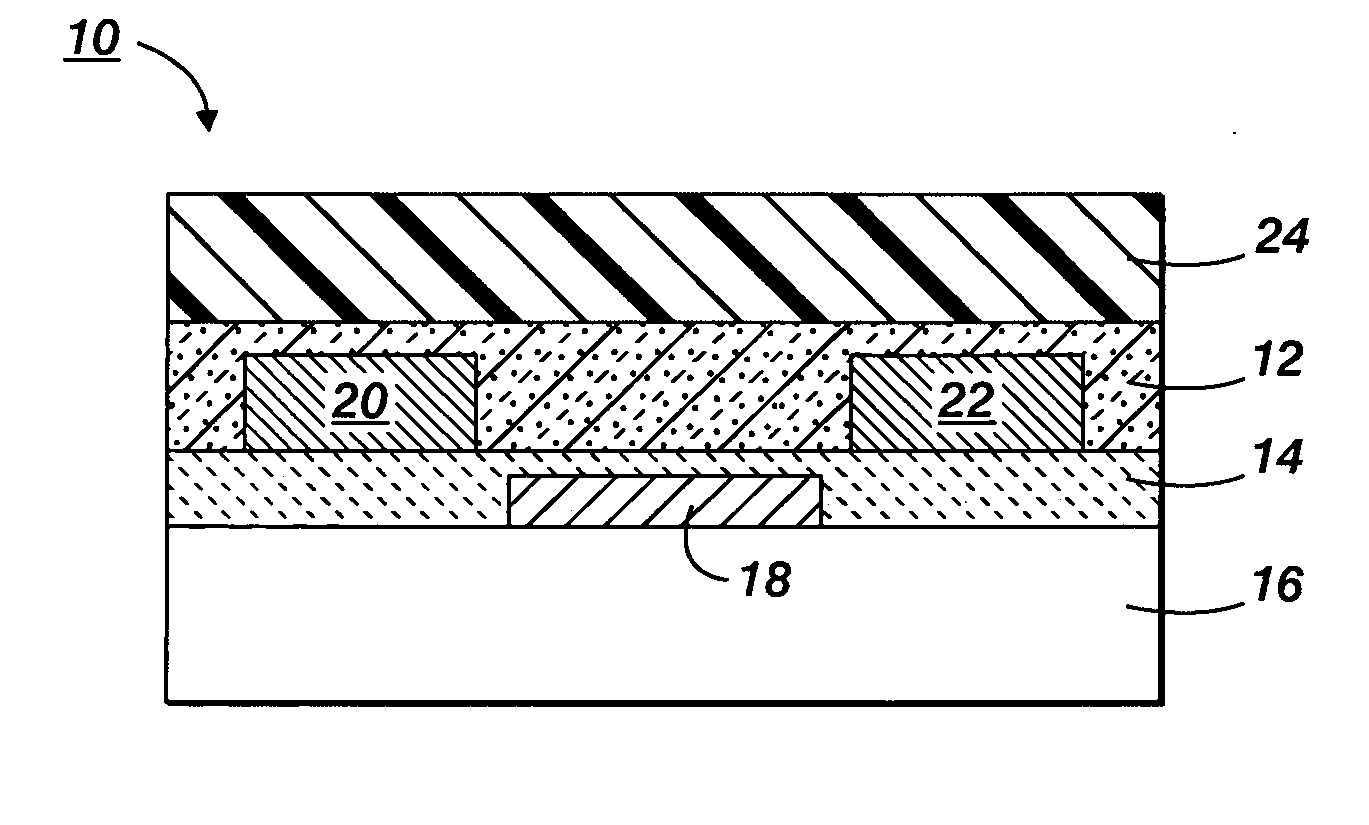
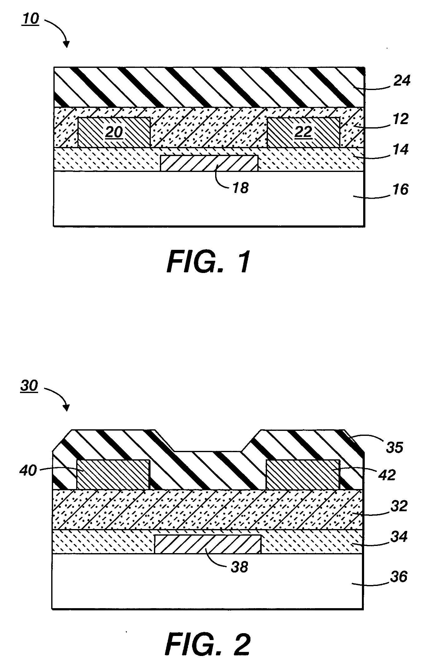
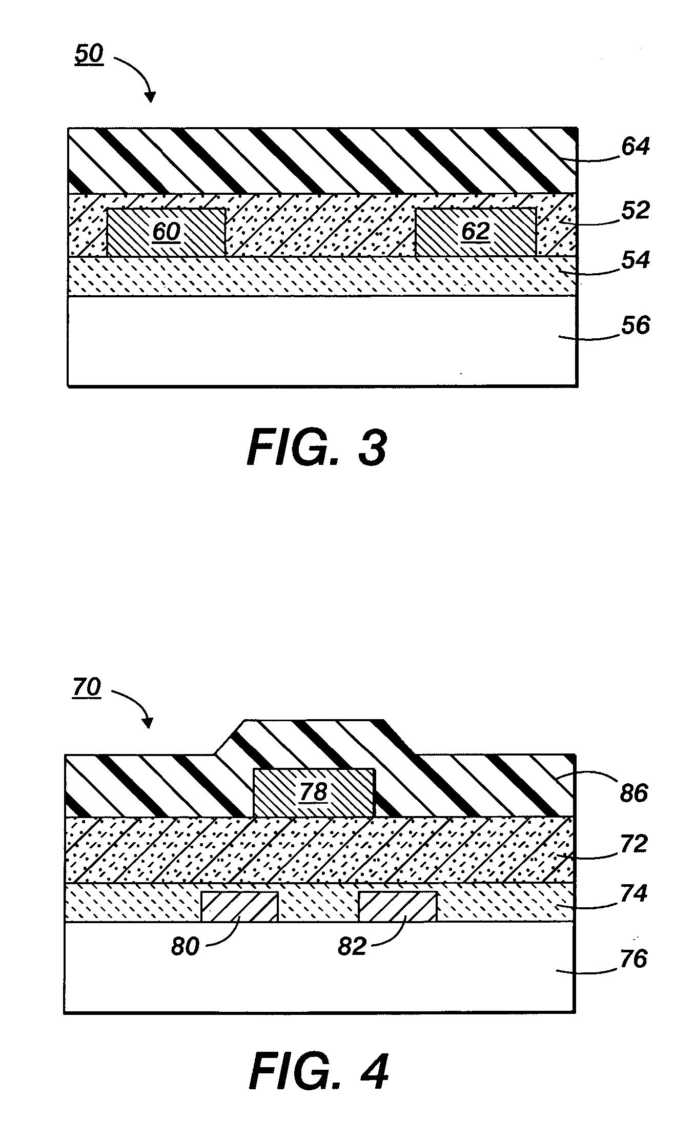
[0078] A top-contact thin film transistor configuration as schematically illustrated, for example, in FIG. 3 was fabricated according to the General Procedure.

[0079] The devices were encapsulated with a POLYWAX 500™ as follows. POLYWAX 500™ was dissolved in heptane at a 0.3 percent by weight with heating to about 80° C. The hot solution was spin coated on top of the devices at 1,000 rpm for 30 seconds. After drying at 60° C., the devices were stored at the same conditions as the control devices. The performance characteristics from at least five of the resulting transistors are summarized in Table 2.

TABLE 2Stability of Organic Thin Film TransistorsWith Wax Composition as Encapsulation LayerTimeMobility (cm2 / V · s)Current On / off ratio 0 day0.06-0.12106˜10715 days0.05-0.10106˜10730 days0.04-0.09106˜1071 and half year0.003104˜105(1.5)

[0080] Generally, the above data illustrates performance improvement and characteristics with a wax coating when two substantially identical thin film ...


PUM


Abstract

An electronic device comprising: a substrate, an active layer, and an encapsulating layer comprising at least one wax.

Description

CROSS-REFERENCE TO RELATED APPLICATIONS [0001] Illustrated in copending applications U.S. Ser. No. 10 / 042,342, Publication No. 2003 / 0160234; U.S. Ser. No. 10 / 042,357, Publication No. 2003 / 0171531; and U.S. Ser. No. 10 / 042,360, Publication No. 2003 / 0166829, the disclosures of which are totally incorporated herein by reference, all titled “Polythiophenes and Devices Thereof” and all filed Jan. 11, 2002; and also illustrated in U.S. Pat. No. 6,621,099, U.S. Pat. No. 6,770,904 and U.S. Pat. No. 6,777,529 are polythiophenes and devices thereof. [0002] The appropriate components, processes thereof and uses thereof illustrated in these copending applications may be selected for the present disclosure in embodiments thereof.BACKGROUND [0003] The present disclosure is generally directed to devices that are encapsulated, and in embodiments contain polythiophenes. More specifically, the present disclosure in embodiments is directed to thin film transistors and similar electronic devices that c...

Claims


Application Information

Patent Timeline
Patent Type & Authority Applications(United States)
IPC IPC(8): H01L23/28H10N10/856
CPCH01L51/0545H01L51/10H01L51/448H01L51/5237H10K10/80H10K10/466H10K30/88H10K59/873H10K50/844
Inventor WU, YILIANGONG, BENG S.LIU, PING
Owner XEROX CORP
Features
  • R&D
  • Intellectual Property
  • Life Sciences
  • Materials
  • Tech Scout
  • Unparalleled Data Quality
  • Higher Quality Content
  • 60% Fewer Hallucinations
Learn More