Gyro vibration piece, gyro sensor, and method of manufacturing gyro vibration piece
- Summary
- Abstract
- Description
- Claims
- Application Information
AI Technical Summary
Benefits of technology
Problems solved by technology
Method used
Image

Examples
first embodiment
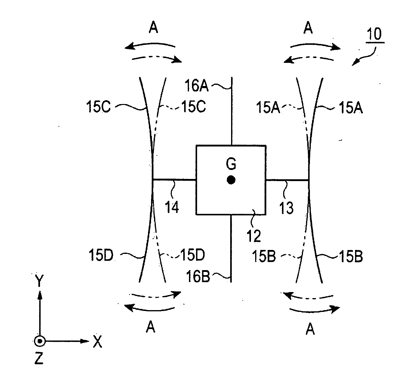
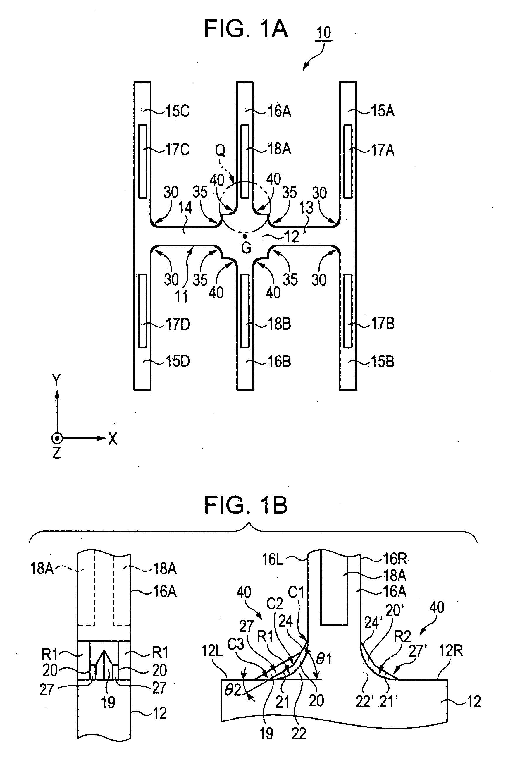
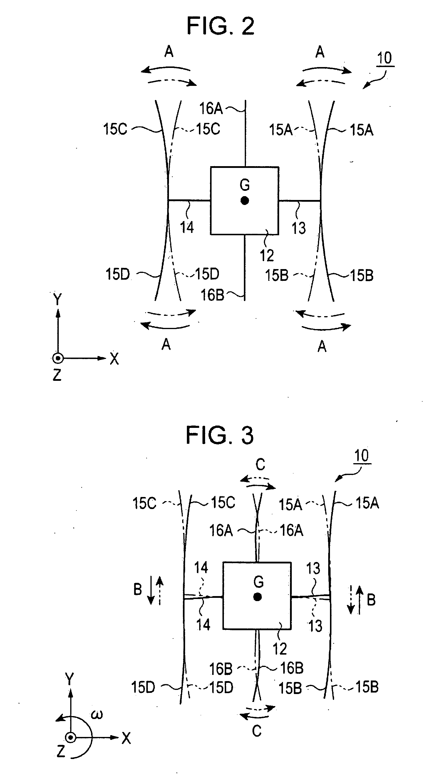
[0039] A gyro vibration piece according to a first embodiment of the present invention will be described with reference to the accompanying drawings. FIG. 1A is a plan view schematically illustrating a structure of a gyro vibration piece according to a first embodiment of the invention, and FIG. 1B is a partially expanded view of Q shown in FIG. 1A and a left-side view thereof.
[0040] In the first embodiment, a double T-type gyro vibration piece will be described as an example of the gyro vibration piece. As shown in FIG. 1A, the gyro vibration piece 10 is formed of a crystal substrate as an example of a piezoelectric substrate. Crystal forming the crystal substrate has an X-axis, which is called an electrical axis, a Y-axis, which is called a mechanical axis, and a Z-axis, which is called an optical axis. The gyro vibration piece 10 is formed in an X-Y plane of Z-cut crystal substrate that is cut in a direction of a plane formed by the X-axis and Y-axis of the crystal. The gyro vib...
second embodiment
[0057] A method of manufacturing a gyro vibration piece according to the present invention will be described with reference to the drawings. FIG. 6 is a process flow of a method of manufacturing a gyro vibration piece. In the second embodiment, a method of forming a gyro vibration piece using a crystal substrate as a piezoelectric substrate will be described.
[0058] A metal layer 51 is formed as a corrosion-resisting film on a surface of a crystal substrate 50. The metal layer 51 is formed of, for example, a chrome (Cr) layer as a base metal, and an aurum (Au) layer as a corrosion-resisting metal formed on the Cr layer. The Cr layer has a thickness of tens of nanometers and the Au layer has a thickness of hundreds of nanometers. The Cr layer having good adherence to the crystal substrate 50 and the Au layer is formed as a base metal layer since the crystal layer 50 has bad adherence to the Au layer. Also, in FIG. 6, the Cr layer and the Au layer are not depicted and a combination of...
third embodiment
[0066] A gyro sensor according to a third embodiment will be described with reference to FIG. 7. FIG. 7 is a front cross-sectional view of the structure of the gyro sensor according to the third embodiment.
[0067] As shown in FIG. 7, the gyro sensor 150 according to the present invention includes a gyro vibration piece 10, supporting arms 151 and 152 of the gyro vibration piece 10 located within a package 154 serving as a holding unit, a supporting substrate 153, and a cover 155 of the package 154.
[0068] The package 154 is formed of, for example, a ceramic. The supporting substrate 153, on which a circuit pattern and the like is formed, is fixed on a hollow formed on a central portion of the package 154. An end portion of each of the supporting arms 151 and 152 is connected to a surface of the supporting substrate 153. The supporting arms 151 and 152 are formed of a flexible metal thin film. The gyro vibration piece 10 is connected to an end portion located on an opposite side of a...
PUM
 Abstract
Description
Claims
Application Information
 - R&D
- Intellectual Property
- Life Sciences
- Materials
- Tech Scout
- Unparalleled Data Quality
- Higher Quality Content
- 60% Fewer Hallucinations
Browse by: Latest US Patents, China's latest patents, Technical Efficacy Thesaurus, Application Domain, Technology Topic, Popular Technical Reports.
© 2025 PatSnap. All rights reserved.Legal|Privacy policy|Modern Slavery Act Transparency Statement|Sitemap|About US| Contact US: help@patsnap.com