Semiconductor device having a dummy gate

a technology of dummy gate and semiconductor device, which is applied in the direction of semiconductor device, semiconductor/solid-state device details, electrical apparatus, etc., can solve the problems of reducing the design rule, the parasitic capacitance between the conductive layer and the interconnect, and the inability to achieve the desired operational speed, etc., to achieve the effect of increasing the flexibility of the arrangement, and increasing the regularity

Active Publication Date: 2006-10-05
MICRON TECH INC
View PDF8 Cites 9 Cited by
  • Summary
  • Abstract
  • Description
  • Claims
  • Application Information

AI Technical Summary

Benefits of technology

[0028] In view of the above, it is an object of the present invention to provide a semiconductor device which includes MOS transistors suitably configured to form an oscillation circuit, and which achieves a high-speed circuit operation and a superior controllability.
[0030] In accordance with the semiconductor device of the present invention, the dummy gate electrode overlying the space between the source of a MOS transistor and the source of the adjacent MOS transistor increases the flexibility in the arrangement of gate electrodes of an electrode group including the normal gate electrodes and dummy gate electrodes. The increase of the flexibility in the arrangement allows the gate electrodes to be arranged with a higher regularity, thereby suppressing the range of variation in the gate width of the gate electrodes, which increases the controllability for the circuit operation, especially in the case where the MOS transistors form a ring oscillator.

Problems solved by technology

While the operational speed of the oscillator circuit has been thus improved, there has occurred a problem in that a desired operational speed cannot be obtained even with the case where a required voltage is applied to the ring oscillator.
This means that the parasitic capacitance between conductive layers and between interconnects cannot be ignored in the recent semiconductor devices which have a smaller and smaller design rule.
Further, along with the increase in the operational speed of the semiconductor device, the oscillation frequency varies widely in some semiconductor devices to cause another problem.
However, along with the reduction in the design rule and the increase in the operational speed of the semiconductor devices, the parasitic capacitance between the drain region 13b and the second-layer drain line 20b causes a substantive problem.
In this configuration, however, flexibility in the arrangement of the gate electrodes is small so that it is difficult to make the interval or pitch between the gate electrodes constant.

Method used


Image

  • Semiconductor device having a dummy gate
  • Semiconductor device having a dummy gate
  • Semiconductor device having a dummy gate

Examples


first embodiment

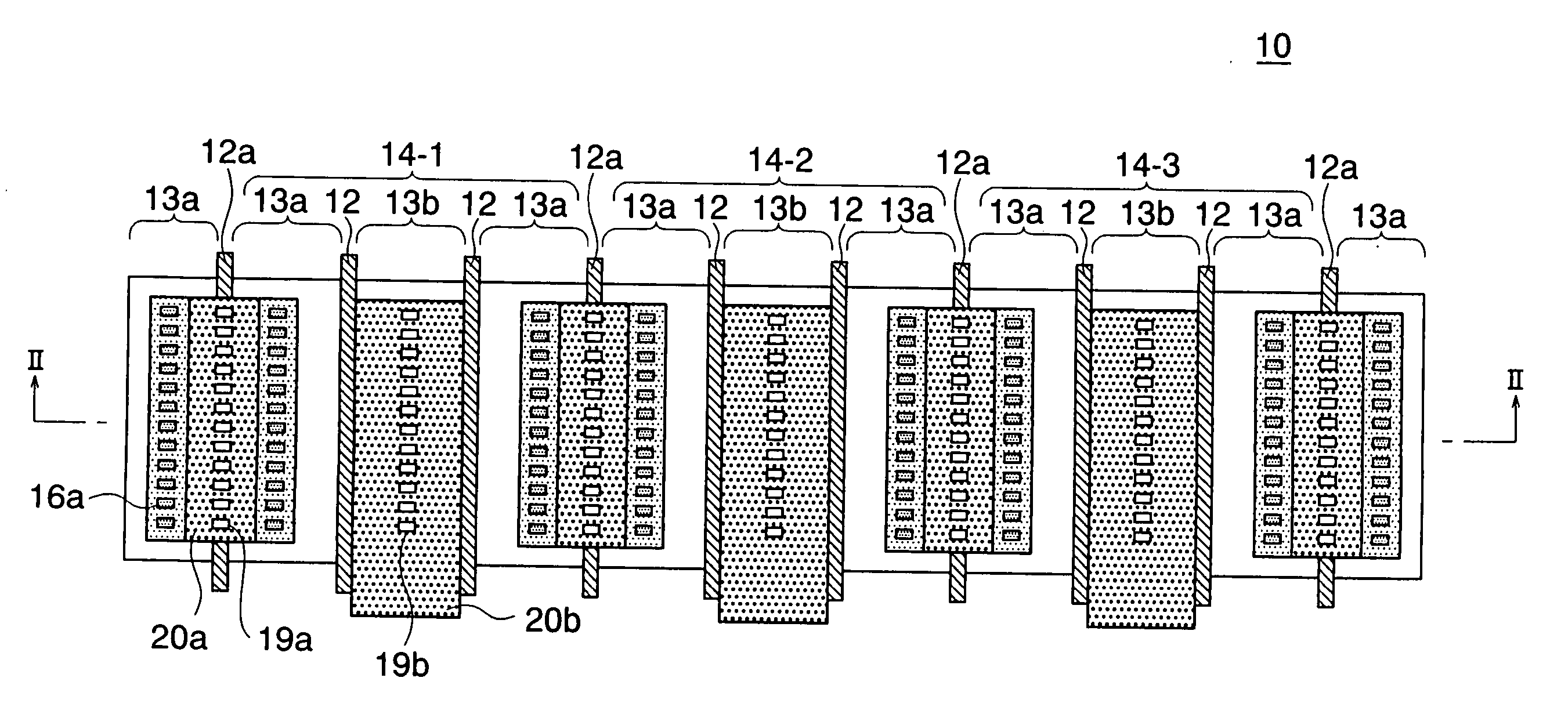
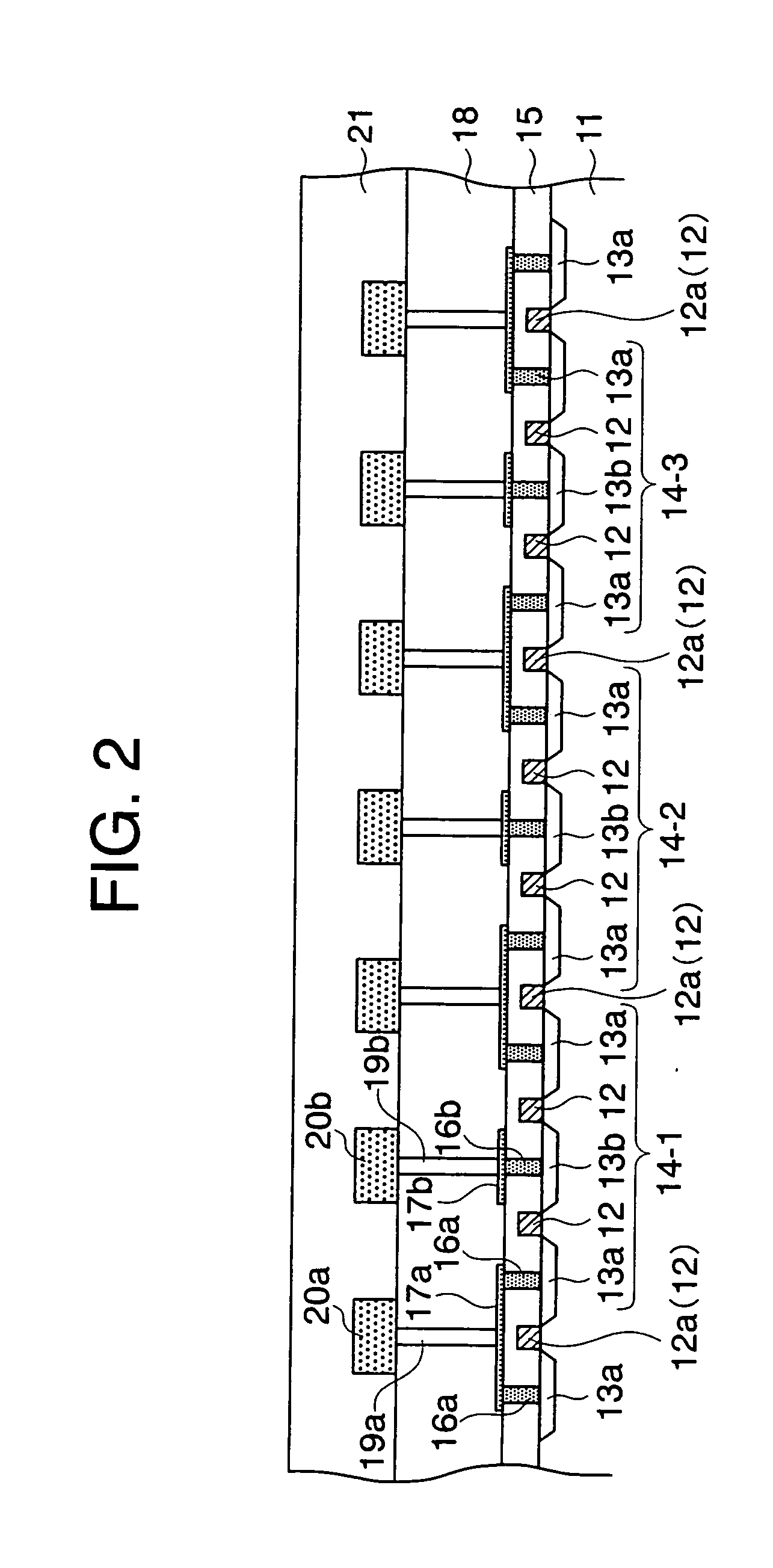
[0051] The present invention will be now described below in further detail with reference to the accompanying drawings. FIG. 1 is a top plan view of a semiconductor device according to the present invention. FIG. 2 is a sectional view taken along line II-II in FIG. 1. In FIG. 2, reference numerals used in the conventional semiconductor device 70 shown in FIGS. 9 and 10 denote the components which are common to the conventional one. Similarly to the semiconductor device 70 shown in FIG. 9, the semiconductor device, generally designated by numeral 10, includes PMOS transistors in the CMOS gates of the ring oscillator 60 such as shown in FIG. 8.

[0052] In the semiconductor device 10, the diffused regions 13 are arranged, starting from a first edge of the semiconductor device 10, in the order of source (source region) 13a, source 13a, drain (drain region)13b, source 13a, source 13a, drain 13b, . . . , drain 13b, source 13a and source 13a, which is disposed at a second edge of the semicon...

second embodiment

[0061]FIG. 4 is a top plan view of a semiconductor device according to the present invention. The semiconductor device, generally designated by numeral 30, includes therein a ring oscillator such as shown in FIG. 8, which includes a PMOS section 31 configured as by the portion of the semiconductor device 10 shown in FIG. 1 and an NMOS section 32 including nMOS transistors 14-1, 14-2, and 14-3 and configured as NMOS transistors. The PMOS section 31 and NMOS section 32 are arranged in parallel to each other in the lengthwise direction, with the pMOS transistors 14-1 to 14-3 of PMOS section 31 and the respective nMOS transistors 14-1 to 14-3 of NMOS section 32 opposing each other.

[0062] The second-layer drain line 20b of the PMOS section 31 extends toward the NMOS section 32 to be connected to the second-layer drain line 20b of the NMOS section 32. Pairs of gate electrodes 12 formed in the pMOS transistors 14-1 to 14-3 of the PMOS section 31 are connected to the counterparts of the NMO...

third embodiment

[0067]FIG. 6 is a top plan view of a semiconductor device according to the present invention. The semiconductor device, generally designated by numeral 40, is similar to the semiconductor device 10 of FIG. 1 except that the second-layer drain line 20b is formed only in the portion in the vicinity of the nMOS section. In the semiconductor device 40 of the present embodiment, the length of the portion in which the second-layer drain line 20b and the second-layer source line 20a extend parallel to each other or the length of the overlapping portion between the second-layer drain line 20b and the first-layer drain line 17b disposed below the second-layer drain line 20b or the underlying drain region 13b is reduced, thereby reducing the parasitic capacitance between them.


PUM


Abstract

A semiconductor device includes a plurality of MOS transistors, wherein each of the MOS transistors has a drain region, a pair of source regions sandwiching therebetween the drain region, and a pair of normal gates each overlying a space between the drain region and a corresponding one of the source regions. A plurality of dummy gates are provided each between adjacent two of the MOS transistors. The dummy gate electrodes are maintained at an equi-potential with the adjacent drain regions. MOS transistors include a row of pMOS transistors and nMOS transistors, wherein each of pMOS transistors and a corresponding nMOS transistor configure a CMOS gate, and a plurality of CMOS gates configure a ring oscillator.

Description

BACKGROUND OF THE INVENTION [0001] 1. Field of the Invention [0002] The present invention relates to a semiconductor device having a dummy gate and, more particularly, to a semiconductor device including a plurality of MOS transistors and a dummy gate disposed between adjacent MOS transistors. [0003] 2. Description of the Related Art [0004] A ring oscillator in a semiconductor device is such that an odd number of inverters are connected or cascaded in a loop. If the inverter is configured by a CMOS gate configured on a semiconductor substrate, such an oscillator circuit can be formed in a small area and is suitably employed in a clock circuit of the semiconductor device. The operational speed of the oscillator circuit has been increased steadily and its oscillation frequency is about to exceed 1 GHz. [0005] While the operational speed of the oscillator circuit has been thus improved, there has occurred a problem in that a desired operational speed cannot be obtained even with the ca...

Claims


Application Information

Patent Timeline
Patent Type & Authority Applications(United States)
IPC IPC(8): H01L29/78
CPCH01L23/5222H01L27/0207H01L27/092H01L2924/0002H01L2924/00
Inventor YOSHIDA, KAZUHIRO
Owner MICRON TECH INC
Why Eureka
Try Eureka