Phase change memory device

a phase change memory and phase change technology, applied in information storage, static storage, digital storage, etc., can solve the problems of reducing cell size and hindering high-speed read operation, and achieve the effects of suppressing the influence of diffusion layer capacitance, reducing reading speed and high-speed read operation

Active Publication Date: 2008-12-25
LONGITUDE LICENSING LTD
View PDF7 Cites 8 Cited by
  • Summary
  • Abstract
  • Description
  • Claims
  • Application Information

AI Technical Summary

Benefits of technology

[0016]As described above, according to the present invention, the memory cell is formed of the phase change element and the diode, and the lower diffusion layer is precharged by the precharge circuit when the memory cell is not selected. Thereby, the diode becomes a reverse-biased state when seeing the memory cell from the bit line so that influence of the diffusion layer capacitance is suppressed. Accordingly, a decrease in reading speed can be prevented by the operation of charging the diffusion layer capacitance during read operation of the memory cell, so that high-speed read operation can be achieved. Further, sufficient write current flowing from the select transistor to the ground line is obtained, and the phase change memory device can be configured in which memory cells are arranged with high density by reducing the cell size.

Problems solved by technology

Therefore, if a MOS transistor is used as a select switch of the phase change element in a case of configuring a memory cell of the phase change memory device, it needs to have a gate width large enough to flow the write current and a reduction in cell size becomes difficult.
Further, when reading out the other memory cell MC during the write operation for the specified memory cell MC on the word line WL, an increase in the potential of the word line WL causes noise and high-speed read operation is hindered.

Method used


Image

  • Phase change memory device
  • Phase change memory device
  • Phase change memory device

Examples


Embodiment Construction

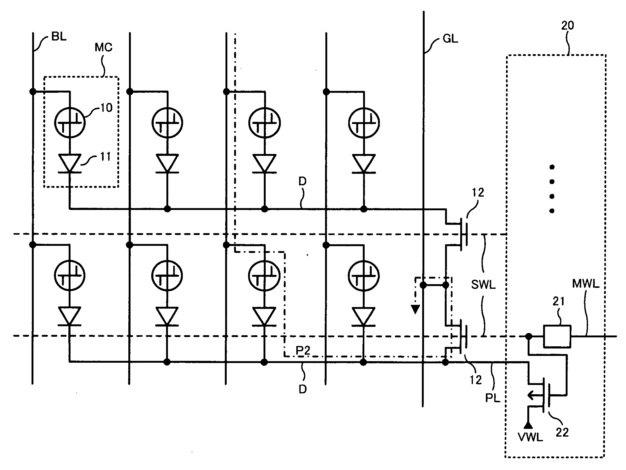
[0026]An embodiment of the present invention will be described below with reference to accompanying drawings. In this embodiment, a case will be described where the present invention is applied to a phase change memory device employing a hierarchical word line structure and rewritably storing data using memory cells each formed of a phase change element and a diode.

[0027]FIG. 1 is a diagram showing a basic circuit configuration of the phase change memory device to which the present invention is applied. In FIG. 1, a large number of memory cells MC are arranged in a matrix form at intersections of sub-word lines SWL and bit lines BL. Further, a select transistor 12 is disposed below the memory cell MC. In the select transistor 12, its gate is connected to the sub-word line SWL, one end of a diffusion layer D is connected to anodes of a plurality of diodes 11, and the other end of the diffusion layer D is connected to a ground line GL arranged in parallel with the bit line BL. Each me...


PUM


Abstract

A phase change memory device comprises: a phase change element for rewritably storing data by changing a resistance state; a memory cell arranged at an intersection of a word line and a bit line and formed of the phase change element and a diode connected in series; a select transistor formed in a diffusion layer below the memory cell, for selectively controlling electric connection between an anode of the diode and a ground line in response to a potential of the word line connected to a gate; and a precharge circuit for precharging the diffusion layer below the memory cell corresponding to a non-selected word line to a predetermined voltage and for disconnecting the diffusion layer below the memory cell corresponding to a selected word line from the predetermined voltage.

Description

BACKGROUND OF THE INVENTION[0001]1. Field of the Invention[0002]The present invention relates to a non-volatile phase change memory device for rewritalbly storing data using a change in resistance state of a phase change element, and particularly relates to a phase change memory device in which a memory cell is formed by connecting the phase change element and a diode in series.[0003]2. Description of the Related Art[0004]A non-volatile semiconductor memory device such as a flash memory becomes more important in recent years. Particularly, attention is paid to a phase change memory device as a promising technique, which uses structural change of phase change material. The phase change memory device has a structure in which a resistance state of a phase change element made of the phase change material is changed by heat and thereby data can be rewritably stored. In a write operation of the phase change memory device, joule heat due to current is generated so as to change the resistan...

Claims


Application Information

Patent Timeline
Patent Type & Authority Applications(United States)
IPC IPC(8): G11C11/00G11C7/00
CPCG11C11/5678G11C13/0004G11C13/0023G11C13/0028G11C13/0069G11C2013/0078G11C2213/72
Inventor NAKAI, KIYOSHITSUKADA, SHUICHIJONO, YUSUKE
Owner LONGITUDE LICENSING LTD
Why Eureka
Try Eureka