
Semiconductor memory device and control method for the semiconductor memory device

a memory device and semiconductor technology, applied in static storage, digital storage, instruments, etc., can solve the problems of inability to record data as multiple-value memory, data in the first page cannot be written in the writing operation in the “reverse direction, and cannot be changed, so as to achieve high-speed reading operation, cost reduction, and speed. the effect of high speed

Inactive Publication Date: 2007-01-11
PANASONIC CORP
View PDF1 Cites 3 Cited by
  • Summary
  • Abstract
  • Description
  • Claims
  • Application Information

AI Technical Summary

Benefits of technology

[0019] Therefore, a main object of the present invention is to realize a writing operation in which data can be written at random addresses in a multiple-value flash memory.

Problems solved by technology

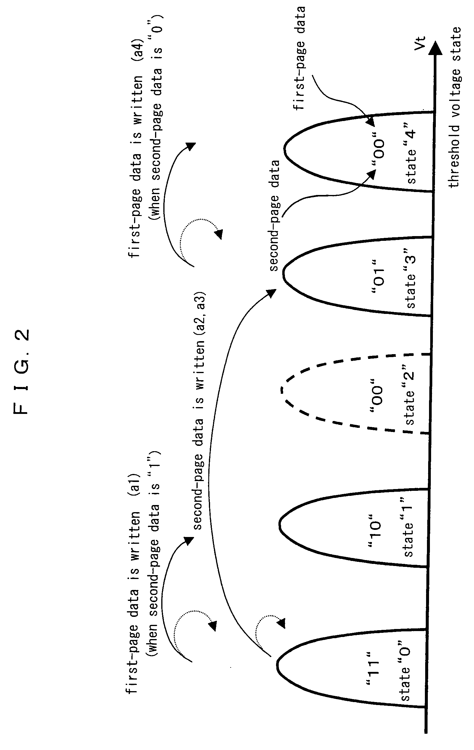
There is a problem that the data writing operation must is executed according to a “forward direction” as first page→second page in the conventional multiple-value memory cells described above.
Therefore, it is not possible to change “3”, which is the highest threshold voltage in the four states in the writing operation, back to “1” or “2”.
Then, the data in the first page cannot be written in the writing operation in the “reverse direction” because there trouble is generated in a sequential shift of the memory cell (threshold voltage).
As a result, the data cannot be recorded as the multiple-value memory.
Due to the disadvantage, the conventional writing operation could be limitedly executed only in the “forward direction”, first page→second page, there has been a problem that it is not possible to write the data in the multiple-value flash memory at random addresses.

Method used


Image

  • Semiconductor memory device and control method for the semiconductor memory device
  • Semiconductor memory device and control method for the semiconductor memory device
  • Semiconductor memory device and control method for the semiconductor memory device

Examples


embodiment 1

Preferred Embodiment 1

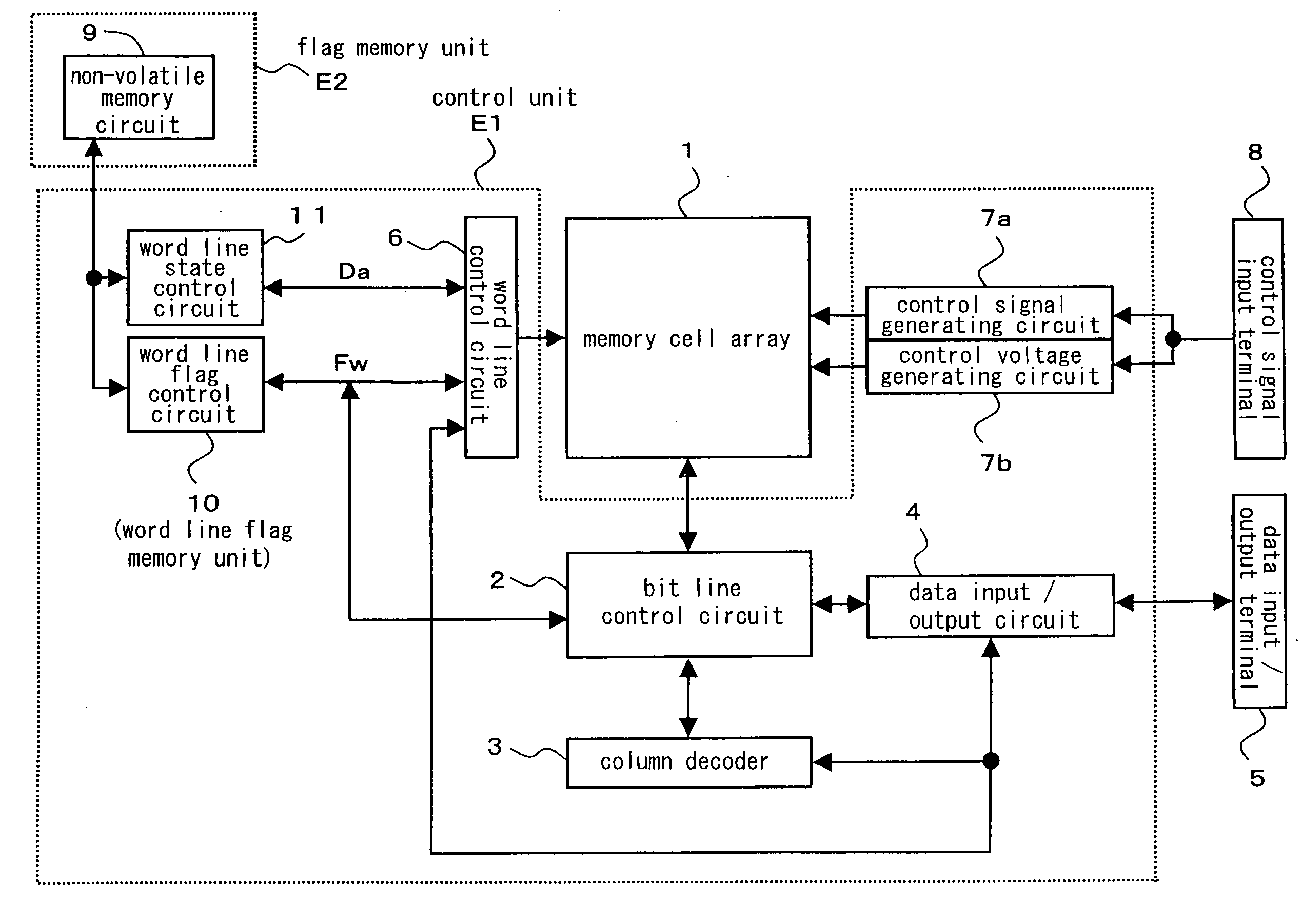
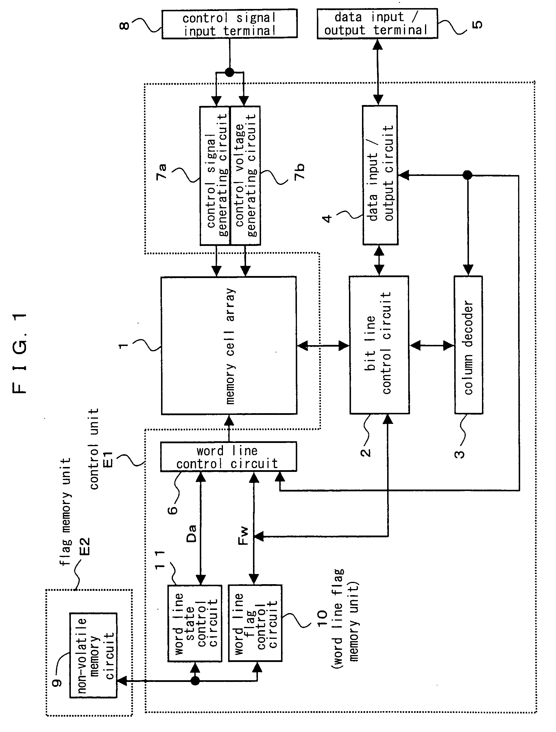
[0100] Referring to a block diagram shown in FIG. 1 which illustrates a constitution of a semiconductor memory device according to a preferred embodiment 1 of the present invention, operations of respective components are described. In FIG. 1, E1 denotes a controlling unit, and E2 denotes a flag memory unit. The controlling unit E1 comprises a bit line control circuit 2, a column decoder 3, a data input / output circuit 4, a word line control circuit 6, a control signal generating circuit 7a, a control voltage generating circuit 7b, a word line flag control circuit 10 and a word line state control circuit 11. The word line flag control circuit 10 corresponds to a word line flag memory unit in which a flag data is memorized ch the fourth, third and first judgment levels are used (S506, S507 and Sfor each word line. The flag memory unit E2 is comprised of a non-volatile memory circuit 9. Any other component, which is same as that of the conventional technology show...

embodiment 2

Preferred Embodiment 2

[0163] A preferred embodiment 2 of the present invention is described referring to a block diagram illustrating a constitution of a semiconductor memory device shown in FIG. 6. The preferred embodiment 2 is different from the preferred embodiment 1 (FIG. 1) in that a volatile memory 12 is provided. The volatile memory 12 is connected to the flag memory unit E2 (non-volatile memory circuit 9) and the control unit E1. The volatile memory 12 is provided between the memory unit E2 and the control unit E1, and transmits and receives writing state data Da and the flag data Fw. In general, a processing speed of the non-volatile memory circuit 9 is slow in the writing and reading operations, while the volatile memory 12 comprising a CMOS circuit is capable of reading and writing the data at a high speed. Therefore, the writing and reading operations executed to the non-volatile memory circuit 9 when the data is written and read to the memory cell array 1 in the preferr...

embodiment 3

Preferred Embodiment 3

[0166] A preferred embodiment 3 of the present invention is described referring to a block diagram illustrating a constitution of a semiconductor memory device shown in FIG. 8. The preferred embodiment 3 (FIG. 8) is different from the preferred embodiment 1 (FIG. 1) in that a chip flag control circuit 13 is provided.

[0167] The chip flag control circuit 13 reads a chip flag data Fc from the non-volatile memory circuit 9 and supplies the read data Fc to the word line control circuit 6. The chip flag control circuit 13 further obtains the flag data Pw of each word line from the word line flag control circuit 10 and a word line state data from the word line state control circuit 11, and judges if it is necessary to update the flag data Fc of each chip. The chip flag control circuit 13 writes the updated flag data Fc of each chip in the non-volatile memory circuit 9. The chip flag control circuit 13 corresponds to a chip flag memory unit for managing a state of the...


PUM


Abstract

A memory cell array for memorizing data with any of 0th through fourth threshold voltages and a flag memory unit for memorizing a flag data showing a chronological sequence relationship between writing operations in which data in first and second pages are respectively written are provided. A controller shifts a state of the memory cell from the 0th state to the 0th or first state in accordance with the data in the first page, and shifts the state of the memory cell to any of the 0th, first, second and third states in accordance with the data in the second page in a “forward” writing operation. The controller shifts the state of the memory cell from the 0th state to the 0th or third state in accordance with the data in the second page, and shifts the state of the memory cell to any of the 0th, first, third and fourth states in accordance with the data in the first page in a “reverse” writing operation. A flag data showing the “reverse” writing operation is then memorized in the flag memory unit.

Description

BACKGROUND OF THE INVENTION [0001] 1. Field of the Invention [0002] The present invention relates to a semiconductor memory device capable of memorizing multiple-value data and a control method for the semiconductor memory device. [0003] 2. Description of the Related Art [0004] A NAND flash memory wherein EEPROM (Electrically Erasable and Programmable Read Only Memory) is used has been proposed as a non-volatile semiconductor capable of electrically rewriting data. In the NAND flash memory, sources and drains of a plurality of memory cells adjacently placed are serially connected, and the multiple memory cells serially connected is connected to a bit line as a unit. In the NAND flash memory, the data is written in and read from all or half of the plural cells placed in a row direction. [0005] Recently, a multiple-value memory for memorizing a plural data in a cell of the NAND flash memory has been developed. No. 2001-93288 of the Publication of the Unexamined Japanese Patent Applica...

Claims


Application Information

Patent Timeline
Patent Type & Authority Applications(United States)
IPC IPC(8): G11C29/00
CPCG11C11/5628G11C16/10G11C16/0483G11C11/5642
Inventor ARITA, MAKOTO
Owner PANASONIC CORP
Learn More