Semiconductor device including trench with at least one of an edge of an opening and a bottom surface being round

Inactive Publication Date: 2006-06-27
MITSUBISHI ELECTRIC CORP
View PDF51 Cites 7 Cited by
  • Summary
  • Abstract
  • Description
  • Claims
  • Application Information

AI Technical Summary

Benefits of technology

[0066]It is therefore an object of the present invention to provide a technique for improving characteristics, particularly an on state voltag

Problems solved by technology

Such configurations of the trench 4 result in a non-uniform thickness of the gate oxide film 9 formed in the trench 4.
Such reduced thickness of the gate oxide film 9 in the trench 4 particularly in the opening portion and bottom of the trench 4 results in gate breakdown position and breakdown voltage failures.
The defects deteriorate the characteristics of channels formed when a predetermine

Method used


Image

  • Semiconductor device including trench with at least one of an edge of an opening and a bottom surface being round
  • Semiconductor device including trench with at least one of an edge of an opening and a bottom surface being round
  • Semiconductor device including trench with at least one of an edge of an opening and a bottom surface being round

Examples


Embodiment Construction

[0091]B. First Fabrication Method

[0092]The first fabrication method is a method of fabricating a gate oxide film in a trench which is different from the background art method.

[0093](b-1) First Preferred Embodiment

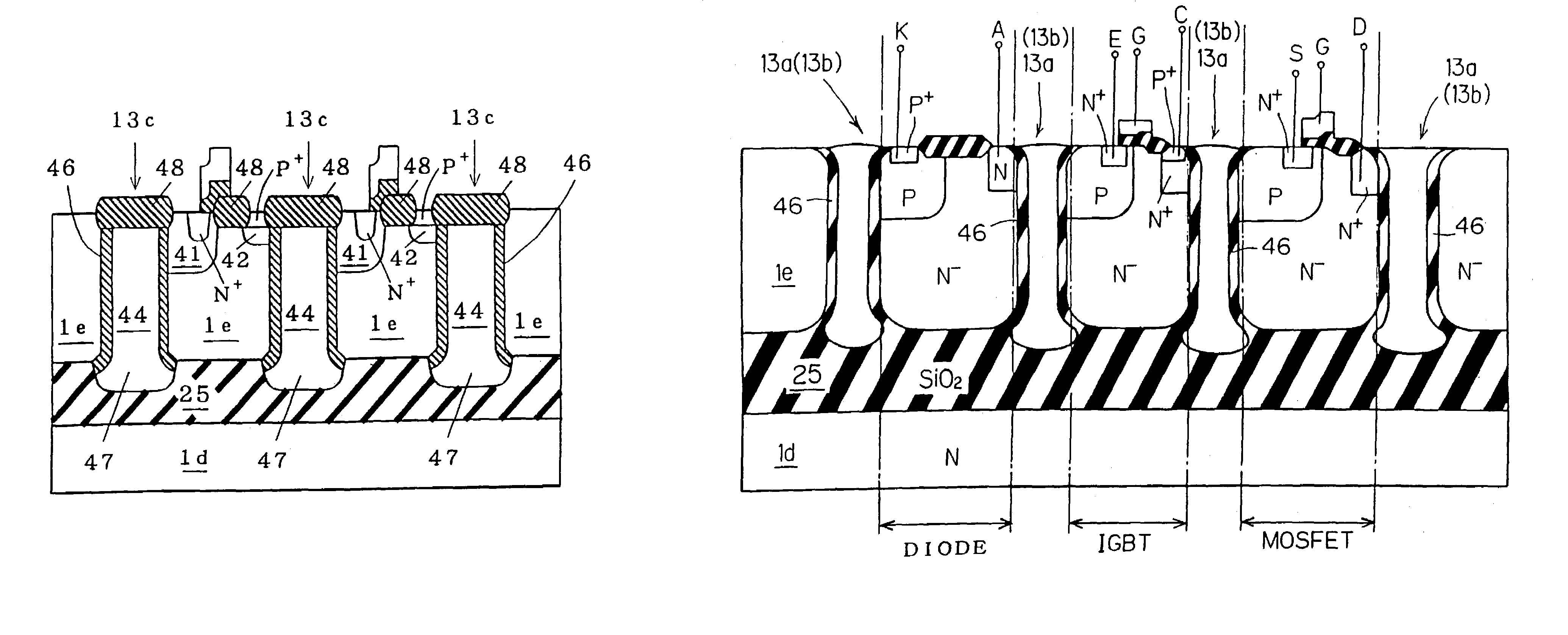
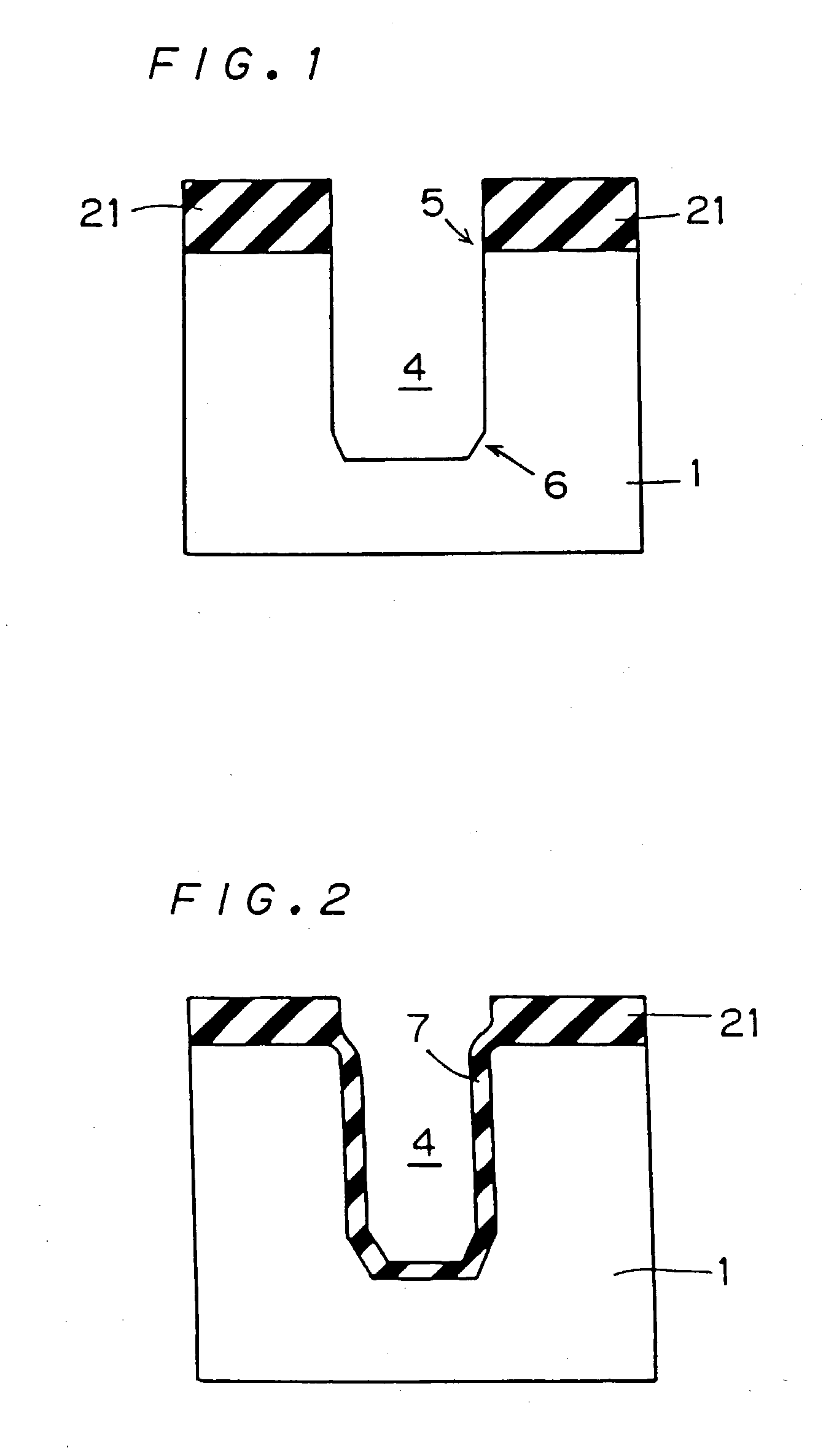
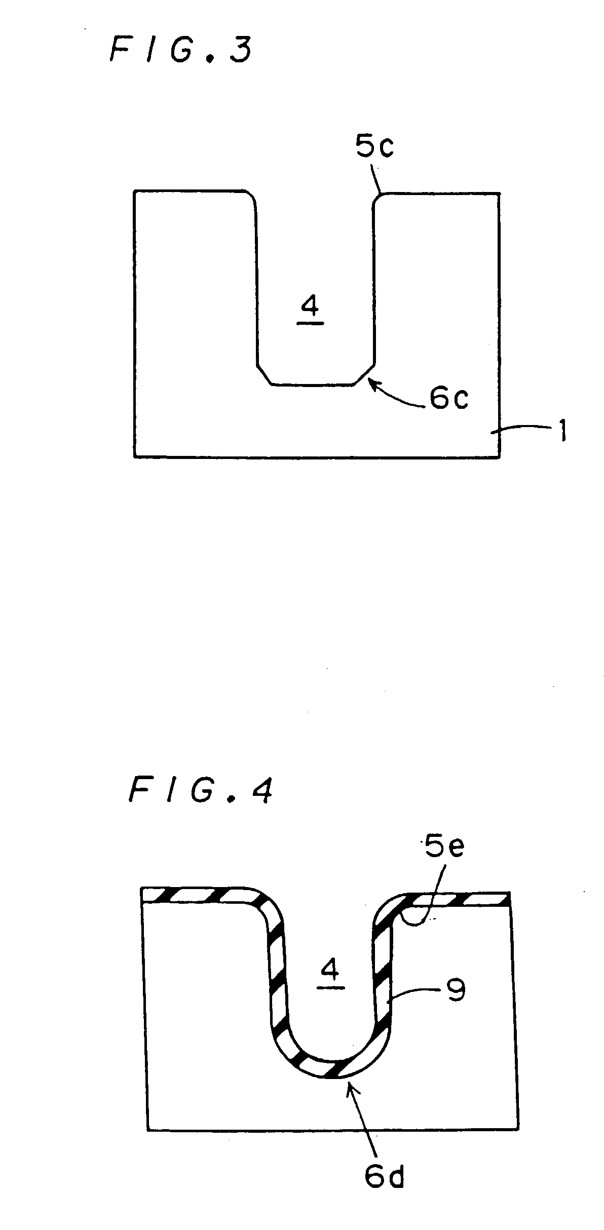
[0094]FIGS. 1 to 5 are cross-sectional views showing a method of forming a trench MOS gate portion 132 in step-by-step fashion according to a first preferred embodiment of the present invention. An oxide film 21 is formed on a substrate 1 made of silicon. An opening is selectively formed in the oxide film 21, and anisotropic silicon etching is performed using the oxide film 21 as a mask to form a trench 4 extending in a direction of the thickness of the substrate 1 (FIG. 1). At this time, an opening portion and a bottom of the trench 4 are of angular configurations 5 and 6, respectively. Then, a sacrificial oxide film 7 of about 100 to 300 nm in thickness is formed in an atmosphere of oxygen at a temperature ranging from 950 to 1100° C., for example, (FIG. 2) and is then re...


PUM


Abstract

A semiconductor device that includes an insulating substrate, a plurality of semiconductor layers arranged to be isolated from one another on the insulating substrate, and a semiconductor element independently provided on the semiconductor layers. Further, a trench may extend from the main surface to the substrate and have an inner wall covered with an insulating film. At least one of an edge on the side of the substrate and an edge on the side opposite thereof of the semiconductor layer has a rounded surface. Further, an angle between a line tangent to a surface having a smallest radius of curvature of the rounded surface of the edge and the main surface ranges from 30° to 60° at a section of the edge.

Description

[0001]This application is a continuation of Ser. No. 09 / 569,031 May 11, 2000 U.S. Pat. No. 6,710,401 which is a continuation of Ser. No. 08 / 996,041 Dec. 22, 1997 U.S. Pat. No. 6,117,734 which is a continuation of Ser. No. 08 / 382,581 Feb. 2, 1995 U.S. Pat. No. 5,783,491.BACKGROUND OF THE INVENTION[0002]1. Field of the Invention[0003]The present invention relates to a technique for forming a trench MOS gate to be applied to a semiconductor device, particularly to a power device. The invention also relates to a device isolation technique.[0004]2. Description of the Background Art[0005]A. Background Art[0006](a-1) First Background Art and Problems thereof[0007]FIGS. 65 to 72 are cross-sectional views showing a conventional process for forming a trench MOS gate portion in step-by-step fashion. In particular, FIG. 72 is a cross-sectional view when a trench MOS gate portion 131 has been formed.[0008]Referring to FIG. 65, a doped P type region 2 is initially formed on an upper surface of a ...

Claims


Application Information

Patent Timeline
IPC IPC(8): H01L29/76H01L29/74H01L21/331H01L21/336H01L21/76H01L21/762H01L21/763H01L29/06H01L29/24H01L29/423H01L29/739H01L29/749H01L29/78H01L29/786H01L29/861
CPCH01L21/76232H01L29/7827H01L21/763H01L29/0696H01L29/4236H01L29/66325H01L29/66348H01L29/66356H01L29/66378H01L29/66666H01L29/7391H01L29/7394H01L29/7397H01L29/7455H01L29/78H01L29/7801H01L29/7813H01L29/7824H01L21/76264H01L21/76286H01L29/1608H01L29/42368
Inventor NAKAMURA, KATSUMIMINATO, TADAHARUTOMINAGA, SHUUICHISHIOZAWA, KATSUOMI
Owner MITSUBISHI ELECTRIC CORP
Why Eureka
Try Eureka