Device for sensing a magnetic field

a magnetic field and sensor technology, applied in the direction of magnetic field magnitude/direction, measurement devices, instruments, etc., can solve the problems of limiting the technical applicability of these magnetic sensors, limiting the maximum achievable flux transfer coefficient, and high sensitivity of “bare” squid not enough for the most demanding

Inactive Publication Date: 2006-10-05
COMMISSARIAT A LENERGIE ATOMIQUE ET AUX ENERGIES ALTERNATIVES +1
View PDF1 Cites 12 Cited by
  • Summary
  • Abstract
  • Description
  • Claims
  • Application Information

AI Technical Summary

Benefits of technology

[0028] The present invention aims at overcoming the above-mentioned drawbacks and in particular at avoiding the use of Hall sensors or SQUIDs whilst allowing the production of a sensing device having comparable or better performances than the known magnetometers.
[0029] The invention further aims at providing a compact and reliable sensor of magnetic flux which is easy to produce and may be used in any magnetic sensor application including biomagnetic detection.
[0030] The invention further aims at improving the sensitivity of the sensing devices for sensing a magnetic field in different applications.
[0042] According to a specific embodiment, the device according to the invention further comprises a negative feed-back loop having a feed-back current driven into an additional coil inductively coupled to the pick-up loop to counteract an external magnetic flux and to thus prevent the appearance of a Meissner current in the pick-up loop.
[0052] It is possible to reduce the 1 / f-noise, by a modulation of the AC current and by choosing a working point for the GMR where the second derivative of R(H) is maximal. In that case, low frequency fluctuations are measured around the second harmonics of the AC frequency. The improvement is the suppression of the 1 / f noise with a decrease of the sensitivity by a factor about 4.
[0053] In the flux gate applications where larger field variations must be dealt with and the extreme fT-level sensitivity is not necessary a smaller size FFDT with a wider constriction can be used. In this way the working range of the sensor can be moved toward higher fields. The dynamic range will stay the same because an FFDT with smaller loop and wider constriction tolerates a higher flux without exceeding the critical current of the constriction.

Problems solved by technology

For classical superconductors Tc is less than 10 K. This cooling requirement, of course, limits the technical applicability of these magnetic sensors.
Even this high sensitivity of the “bare” SQUID is not sufficient for the most demanding applications like biomagnetism, for example.
Typically, this results in Lft=200 nH, which means a rather large inductance mismatch between the flux transformer and the SQUID, thus limiting the maximal achievable flux transfer coefficient to as low as 7*10−3.
The SQUID-based sensors of the prior art utilizing low temperature superconductors, like niobium, have an excellent noise performance, but the cryogenics technology required for cooling the sensors to the working temperature below Tc is expensive and may even be impossible to implement in some applications.
Cooling a geomagnetic flux-gate to liquid helium temperature every time the device is used in the field is not practical.
The problems with the high-Tc SQUID technology are associated with the low yield, lack of chemical stability, and high price of the high-Tc SQUIDs.
Efficient mass production of high-Tc SQUIDs is difficult because of the techniques used in making the weak links necessary for the quantum interference phenomenon.
Whereas the weak links in the niobium SQUIDs are simply realized by a thin insulator layer between two niobium layers on top of each other similar multilayer structures of high-Tc material have turned out to be difficult to make.
The lack of multilayer high-Tc technology also prevents the fabrication of efficient multi-turn fluxtransformers.

Method used


Image

  • Device for sensing a magnetic field
  • Device for sensing a magnetic field
  • Device for sensing a magnetic field

Examples


Embodiment Construction

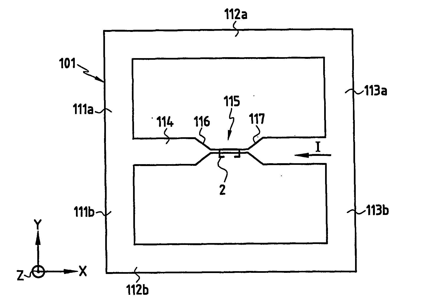
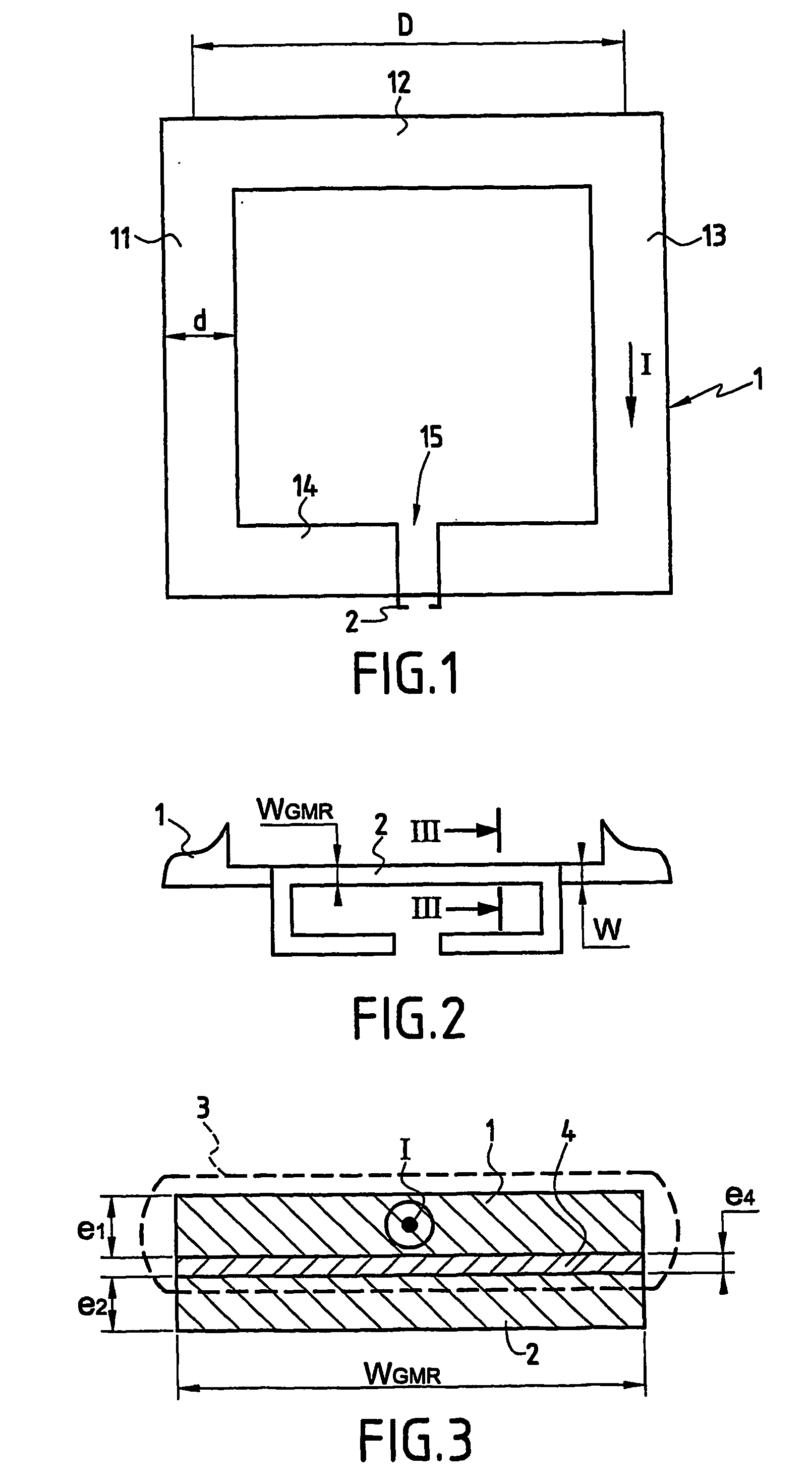
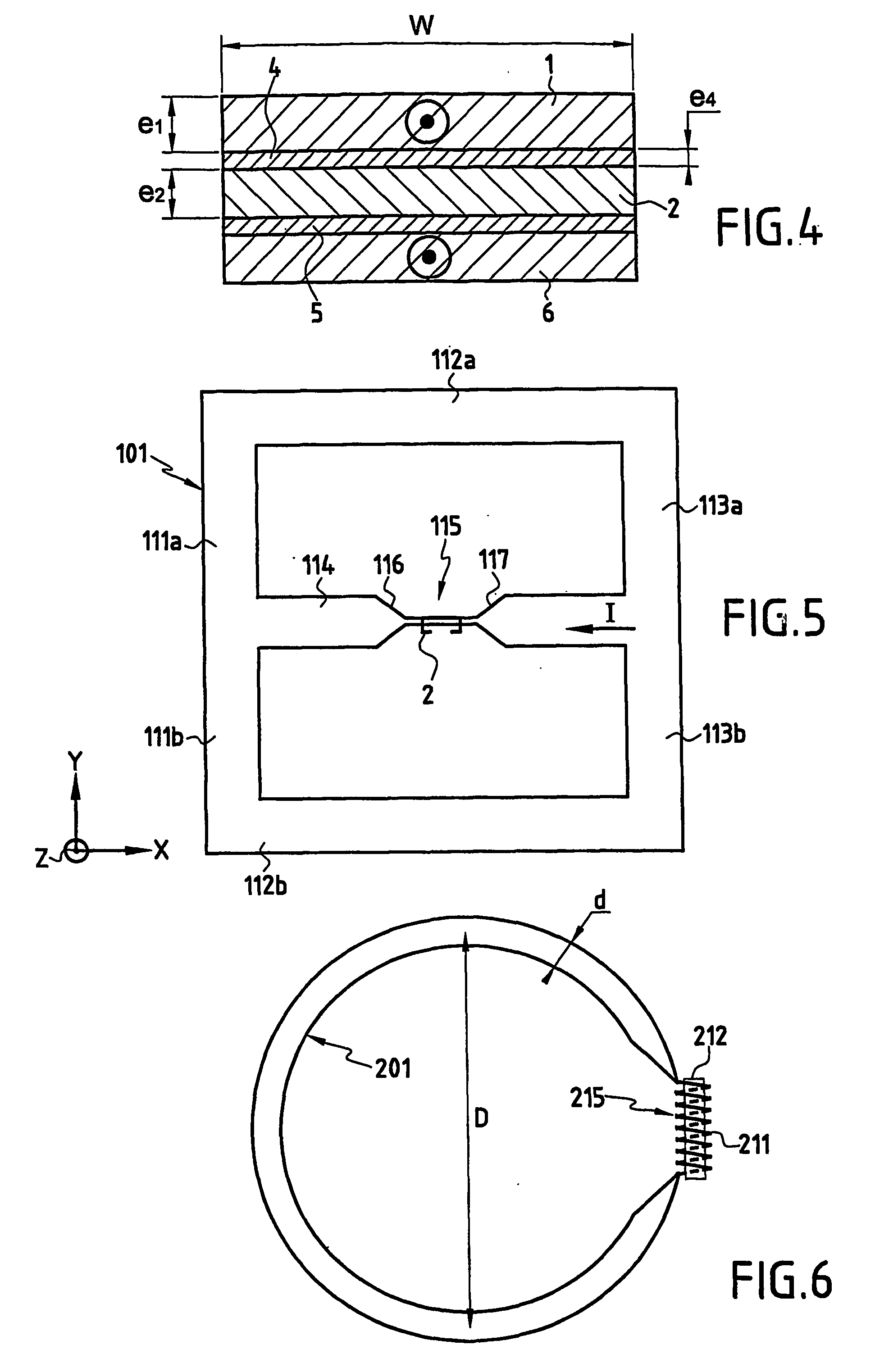
[0063] The physical working principle and basic design of a magnetic sensor based on the present invention is shown in FIG. 1. The superconducting flux guide 1 consists of a square shaped closed loop lithographically etched out of, for example, a high-Tc superconductor thin film. The loop comprises a circumferential path with a first branch 12, two lateral branches 11, 13 and a fourth branch 14 which is parallel to the first branch 12.

[0064] A change ΔB in the magnetic field component perpendicular to the plane of the loop 1 induces a change ΔI in the persistent current I circulating in the loop 1. The magnitude of ΔI is determined by the requirement that the total flux through the closed superconducting loop stays constant (Meissner effect). Therefore, ΔI=ΔB*AFFDT / LFFDT, where AFFDT and IFFDT are the surface area and inductance of the loop 1.

[0065] The inductance of a square shaped loop of superconducting thin film is LFFDT=(μ0 / 2π)*D*[Ln(4D / d)−2.351 (see FIG. 1). To simplify the ...


PUM


Abstract

The device for sensing a magnetic field comprises a closed superconducting pick-up loop (1) having a path width (d) etched out of a single layer superconducting thin film and provided with a constriction (15) having a width (w) of narrow dimension smaller than the path width (d). The closed superconducting pick-up loop (1) constitutes a flux-to-field transformer (FFDT). At least one magnetoresistive element (2) is placed on top of or below the superconducting thin film, is isolated from the superconducting thin film by a thin insulating layer and is located so that an active part of the magnetoresistive element (2) is at the location of the constriction (15) and has a width equal to or less than the width of the constriction (15). The active part of the magnetoresistive element (2) is oriented so that the bias current in this active part is directed essentially along the constriction (15), orthogonally to the width of narrow dimension.

Description

FIELD OF THE INVENTION [0001] The invention relates to a device for sensing a magnetic field. [0002] More specifically, the invention relates to a sensor of magnetic flux using a superconducting pick-up loop. [0003] Thus the sensor can be used in any magnetic sensor application where the cooling of the sensor to below the superconducting transition temperature Tc of the superconducting loop is possible. Description of the Related Art [0004] Magnetic sensors are routinely used in many technical applications such as position, velocity, acceleration, and angle detectors, for example. There is a large variety of magnetic sensor types based on different physical principles. The prior art relevant to the present invention comprises two kind of sensors: magnetoresistive (MR) sensors, and sensors based on superconductivity and SQUIDs (Superconducting Quantum Interference Device). Sensors based on magnetoresistive elements IRE) are compact and easy to use with very simple read-out electronic...

Claims


Application Information

Patent Timeline
Patent Type & Authority Applications(United States)
IPC IPC(8): G01R33/02G01R33/035
CPCG01R33/035
Inventor PANNETIER, MYRIAMFERMON, CLAUDESIMOLA, JUHA
Owner COMMISSARIAT A LENERGIE ATOMIQUE ET AUX ENERGIES ALTERNATIVES
Why Eureka
Try Eureka