Semiconductor device

a technology of semiconductor lasers and semiconductors, applied in semiconductor lasers, laser details, electrical equipment, etc., can solve the problems of difficult reduction, increased noise, power loss of input and output light, etc., and achieve the effect of reducing output power, low cost, and reducing noise characteristics

Active Publication Date: 2006-10-05
FUJITSU LTD
View PDF12 Cites 10 Cited by
  • Summary
  • Abstract
  • Description
  • Claims
  • Application Information

AI Technical Summary

Benefits of technology

[0013] However, in this configuration, although the cost can be reduced, insertion loss of the photodetectors results in power loss of the input and output light, which is difficult of being reduced.
[0018] The present invention has been devised in view of such problem, and aims to provide a semiconductor device allowing a photodetector to be integrated without causing any power loss at a low cost.
[0020] A semiconductor device according the present invention has therefore an advantage of allowing a photodetecor to be integrated without causing any power loss at a low cost.
[0021] For this reason, when a photodetector is integrated with, for example, a semiconductor optical amplifier, the noises characteristic deterioration caused by provision of a photodetector on the input side of a semiconductor optical amplifier can be prevented, and the decrease in output power caused by provision of a photodetector on the output side of the semiconductor optical amplifier can be prevented.
[0022] In particular, since a photodetector is provided in a region other than a region where a semiconductor optical waveguide at least partly capable of functioning as a semiconductor optical amplifier is provided, even in the event of excessively large power of input light or output light, the deterioration of the waveform quality such as waveform distortion by the saturation of the photodetector can be prevented. Furthermore, even in the event of excessively large input light or output light, a detection error (measurement error) can be prevented from occurring.

Problems solved by technology

However, in this configuration, although the cost can be reduced, insertion loss of the photodetectors results in power loss of the input and output light, which is difficult of being reduced.
An increase in power loss of the input light causes an increase in noise figure, thereby deteriorating the noise characteristic.
On the other hand, an increase in power loss of the output light results in a decrease in output power.
Furthermore, too large power of the input light or output light inputted to the photodetector results in deterioration of waveform quality such as waveform distortion due to the saturation of the photodetector.
In addition, there is a fear of bringing about a detection error (measurement error).

Method used


Image

  • Semiconductor device
  • Semiconductor device
  • Semiconductor device

Examples


first embodiment

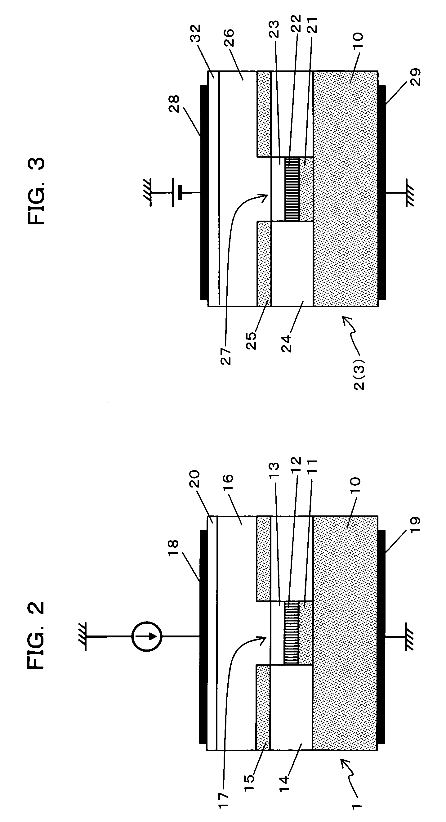
[0036] At first, a semiconductor device according to the first embodiment will be described with reference to FIGS. 1 to 3.

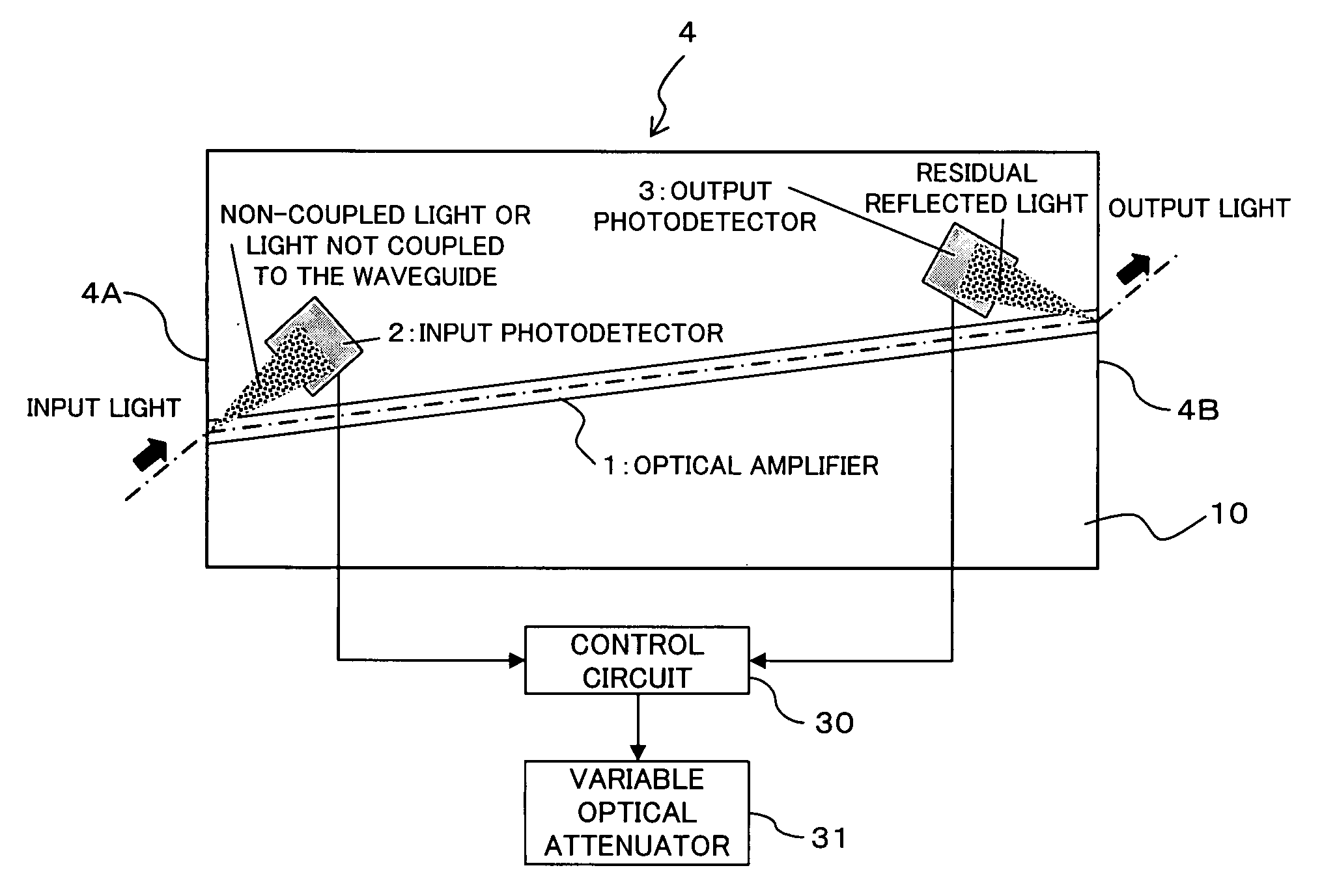
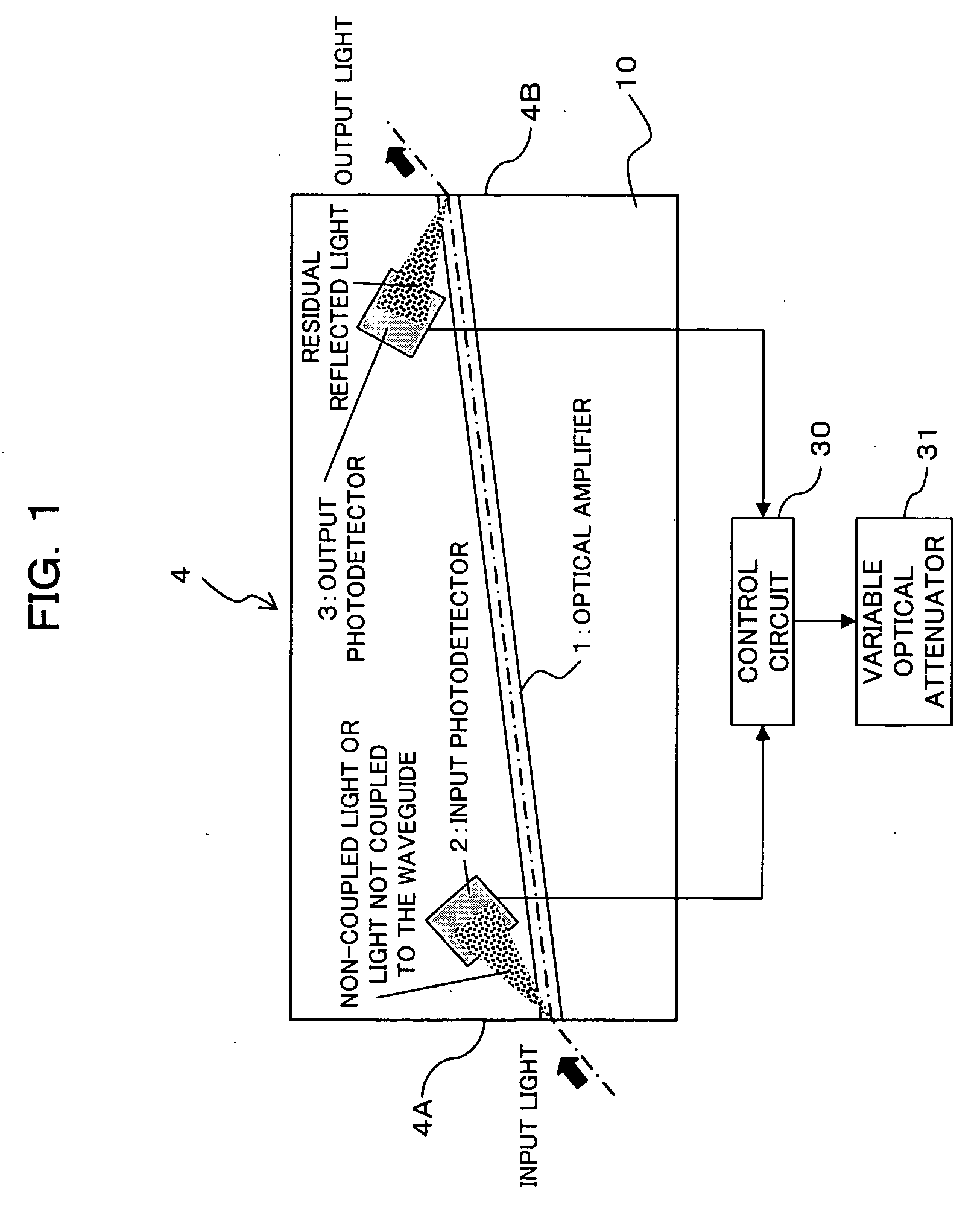
[0037] The semiconductor device according to this embodiment is configured, as shown in FIG. 1, as a semiconductor optical amplifying device (in-line power monitor integrated semiconductor optical amplifier) 4 in which a semiconductor optical amplifier (SOA) 1 and photodetectors 2 and 3 are monolithically integrated.

[0038] Specifically, as shown in FIG. 1, the structure of the semiconductor optical amplifying device 4 is such that there are integrated on a semiconductor substrate 10 a semiconductor optical amplifier (SOA) 1 for amplifying input light and outputting it as output light, an input photodetector 2 for detecting light not-coupled to the waveguide to monitor the power of the input light, and an output photodetector 3 for detecting residual reflected light to monitor the power of the output light.

[0039] In this embodiment, the semiconductor optical a...

second embodiment

[0061] Next, a semiconductor device according to the second embodiment of the present invention will be described with reference to FIG. 4.

[0062] The semiconductor device according to this embodiment differs from the first embodiment described above in that it is provided with a light absorbing region.

[0063] In other words, in this semiconductor device, in addition to the first embodiment described above, as shown in FIG. 4, a light absorbing region 40 capable of absorbing non-guided radiated light (leakage light) from the wall face of the semiconductor optical waveguide without being guided by the semiconductor optical waveguide constituting the semiconductor optical amplifier 1 is provided between the semiconductor optical waveguide constituting the semiconductor optical amplifier 1 and the photodetectors 2 and 3. For this reason, the detection error (measurement error) caused by radiated light (leakage light) from the wall face of the semiconductor optical waveguide constitutin...

third embodiment

[0067] Next, a semiconductor device according to the third embodiment of the present invention will be described with reference to FIG. 5.

[0068] The semiconductor device according to this embodiment differs from the first embodiment described above in that it is provided with optical waveguides for guiding light to the photodetectors.

[0069] In other words, in this semiconductor device, in addition to the first embodiment described above, as shown in FIG. 5, an optical waveguide for detecting input light (optical waveguide for monitoring) 41 is formed between an input side portion of the semiconductor optical waveguide constituting the semiconductor optical amplifier 1 and the input photodetector 2 such that non-guided radiated light from the wall face of the semiconductor optical waveguide constituting the semiconductor optical amplifier 1 is guided to the input photodetector 2 on the input side. In FIG. 5, identical notations are attached to the elements similar to those in FIG. ...


PUM


Abstract

In a semiconductor device comprising a semiconductor optical amplifier, in order to allow a photodetector to be integrated without causing power loss at a low cost, the semiconductor device comprises a semiconductor substrate, a semiconductor optical waveguide, at least partly capable of functioning as a semiconductor optical amplifier, to guide signal light, and a photodetector provided in a region other than a region where the semiconductor optical waveguide is provided, wherein the semiconductor optical waveguide and the photodetector are integrated on the semiconductor substrate.

Description

CROSS REFERENCE TO RELATED APPLICATIONS [0001] This application is based on and hereby claims priority to Japanese Application No. 2005-102946 filed on Mar. 31, 2005 in Japan, the contents of which are hereby incorporated by reference. BACKGROUND OF THE INVENTION [0002] (1) Field of the Invention [0003] The present invention relates to a semiconductor device suitable for use as a semiconductor optical amplifier employed in, for example, an optical communication system. [0004] (2) Description of Related Art [0005] Along with the recent remarkable increase in communication demand, the development of a wavelength division multiplex (WDM) communication system allowing large capacity transmission with one optical fiber by multiplexing a plurality of signal lights of different wavelengths has been progressed. [0006] As an optical amplifier used in such an optical communication system, a semiconductor optical amplifier (SOA) which has a wide wavelength band and a small size and is capable ...

Claims


Application Information

Patent Timeline
Patent Type & Authority Applications(United States)
IPC IPC(8): H01S3/00H01S5/50
CPCH01S5/026H01S5/0262H01S5/1085H01S5/0264H01S5/2206H01S5/227H01S5/50H01S5/2022
Inventor AKIYAMA, TOMOYUKI
Owner FUJITSU LTD
Why Eureka
Try Eureka