Pre-charge Voltage Supply Circuit of Semiconductor Device

Active Publication Date: 2006-10-05
SK HYNIX INC
View PDF10 Cites 132 Cited by
  • Summary
  • Abstract
  • Description
  • Claims
  • Application Information

AI Technical Summary

Benefits of technology

[0006] A pre-charge voltage supply circuit of a semiconductor device is capable of reducing the amount of current leaked through a region where a bridge is formed between a bit line and a word line in association with a pa

Problems solved by technology

The formation of the bridge between the word line and the bit line is mainly caused by a gate residue, namely, poly-silicon remaining without being completely removed after etching of a poly-silicon film to form a gate, or undesirable removal of a nitride film on the gate during a chemical mechanical polishing (CMP) process, and thus, weakness of the corresponding region.
Thus, undesirable current leakage is generated between the word line and the bit line in the standby mode.
In this case, however, t

Method used


Image

  • Pre-charge Voltage Supply Circuit of Semiconductor Device
  • Pre-charge Voltage Supply Circuit of Semiconductor Device
  • Pre-charge Voltage Supply Circuit of Semiconductor Device

Examples


Embodiment Construction

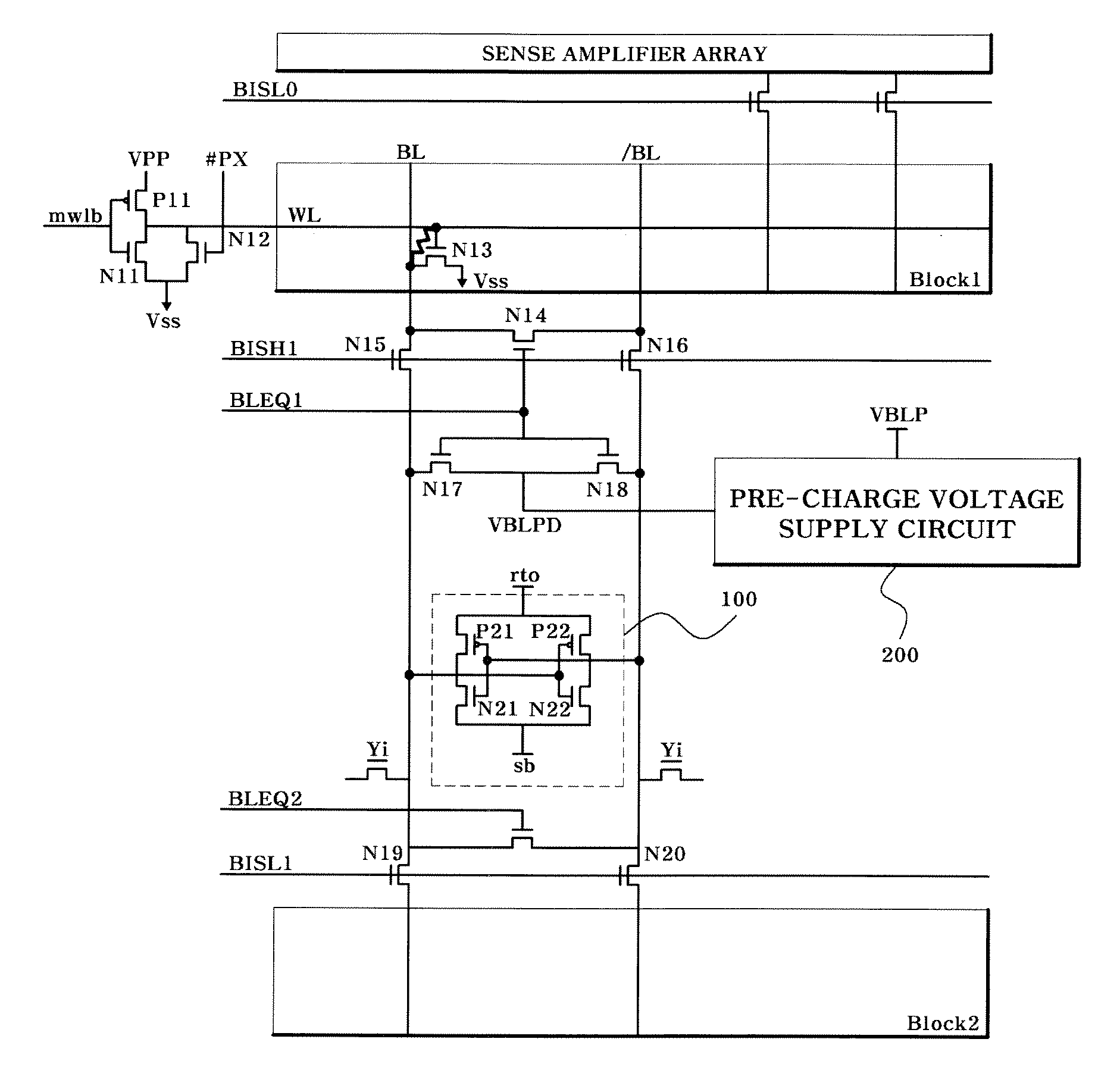
[0032] Hereinafter, the present invention will be described in detail, in conjunction with exemplary embodiments. These embodiments are used only for illustrative purposes, and the present invention is not limited thereto.

[0033] As shown in FIGS. 3 and 4, a pre-charge voltage supply circuit 200 of a semiconductor device may include an n-channel metal oxide semiconductor (NMOS) transistor N100 which supplies a pre-charge voltage VBLP in response to a first signal VPP having a high voltage level, and has a turn-on resistance of a predetermined level, and an NMOS transistor N200 which is connected in parallel to the NMOS N100, supplies the pre-charge voltage VBLP in response to a second signal sa, and has a turn-on resistance lower than that of the NMOS N100. The pre-charge voltage supply circuit 200 may also include a switching controller 300 which receives a third signal ba disabled in response to input of an active command and enabled in response to input of a pre-charge command, a...


PUM


Abstract

A pre-charge voltage supply circuit of a semiconductor device is disclosed which includes a first switch which supplies a pre-charge voltage in response to a first signal having a predetermined voltage level, and has a turn-on resistance of a predetermined level, and a second switch which is connected in parallel to the first switch, supplies the pre-charge voltage in response to a second signal, and has a turn-on resistance lower than the turn-on resistance of the first switch.

Description

FIELD OF THE INVENTION [0001] The present invention relates to a pre-charge voltage supply circuit of a semiconductor device, and, more particularly, to a pre-charge voltage supply circuit of a semiconductor device which is capable of reducing the amount of current leaked through the region where a bridge is formed between a bit line and a word line in association with a particular cell in the semiconductor device, in a standby mode, and rapidly supplying a pre-charge voltage to the bit line and a complementary bit line in a pre-charge mode, thereby achieving an increase in pre-charge speed. DESCRIPTION OF THE RELATED ART [0002] Recently-developed, highly integrated semiconductor devices have a reduced element area. In particular, in the case of a dynamic random access memory (DRAM) device, there is an increased possibility of a phenomenon where a bridge is formed between a bit line and a word line in the process of manufacturing the semiconductor device due to a reduction in the pi...

Claims


Application Information

Patent Timeline
IPC IPC(8): G11C7/00
CPCG11C11/4094G11C7/12G11C7/1048G11C11/4074H03K19/0185
Inventor PARK, SANG ILLEE, JONG WON
Owner SK HYNIX INC
Why Eureka
Try Eureka