Magnetic oscillating device

a technology of magnetic oscillating device and magnetic sensor, which is applied in the field of magnetic oscillating device and magnetic reproducing apparatus, can solve the problems of low output, leakage flux amount, and small size of recording bits

Active Publication Date: 2006-10-05
KK TOSHIBA
View PDF5 Cites 35 Cited by
  • Summary
  • Abstract
  • Description
  • Claims
  • Application Information

AI Technical Summary

Benefits of technology

[0009] A magnetic oscillating device according to an aspect of the present invention comprises: a first magnetic resonance layer with a first magnetic resonance frequency f1; a second magnetic resonance layer with a second magnetic resonance frequency f2 higher than the first magnetic resonance frequency f1; a nonmagnetic layer sandwiched between the first magnetic resonance layer and the sec

Problems solved by technology

However, increase in the density of magnetic recording medium has increasingly reduced the size of recording bits and thus the amount of leakage flux, that is, the amount of signal field, from recording bits.
Under the circumstances, to develop a novel element that can sensitively detect a signal field in a high SNR even with a reduced field becomes a major technical challenge.
However, since the magnetizatio

Method used


Image

  • Magnetic oscillating device
  • Magnetic oscillating device
  • Magnetic oscillating device

Examples


example 1

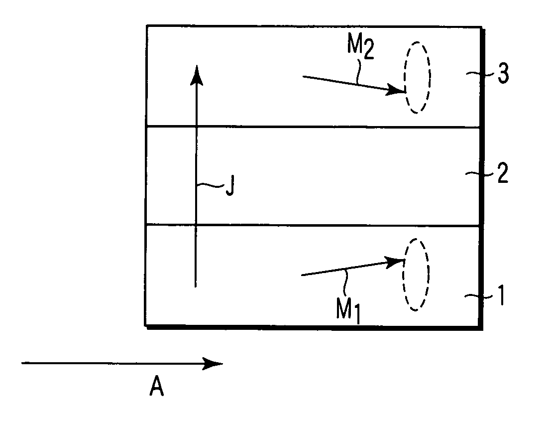
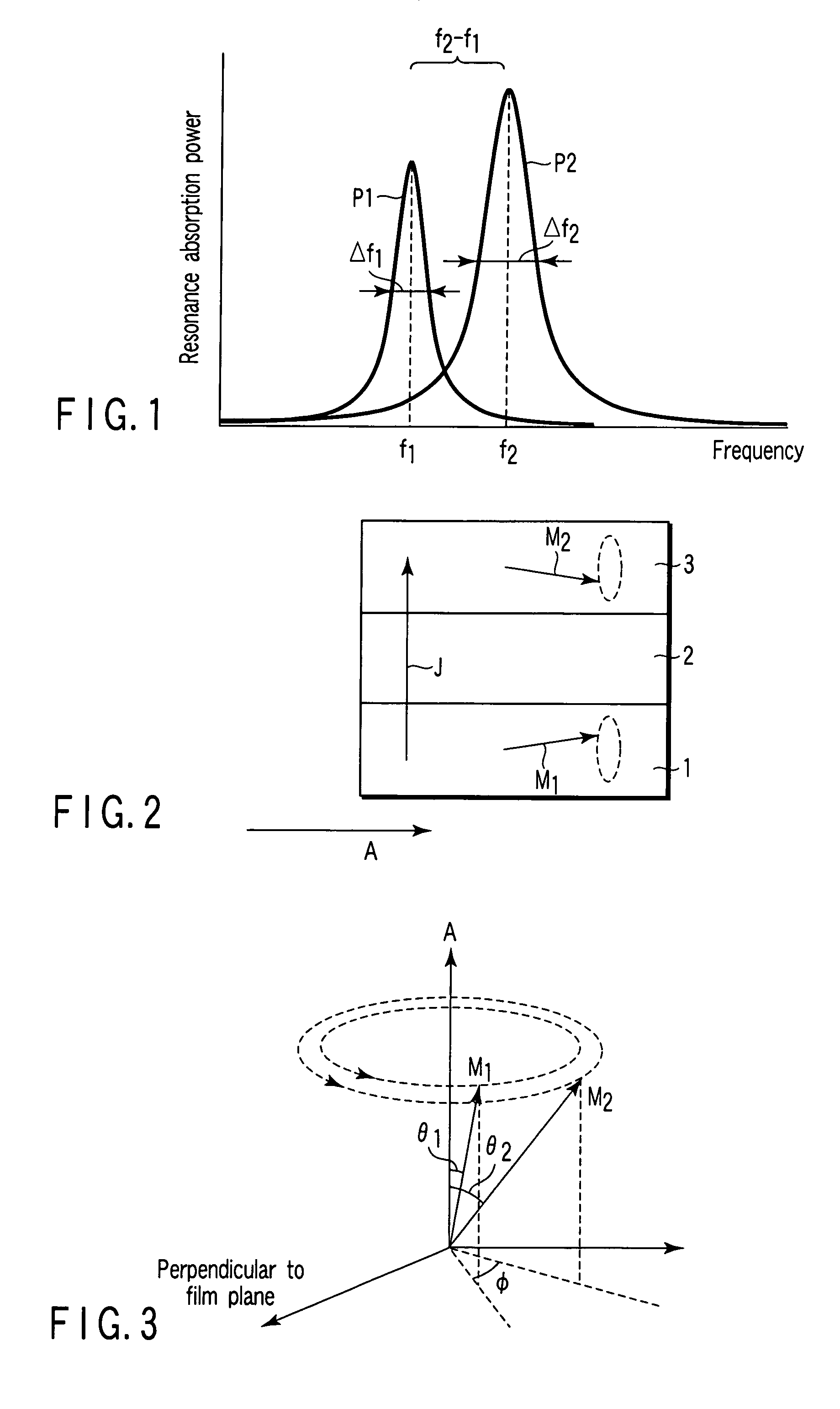
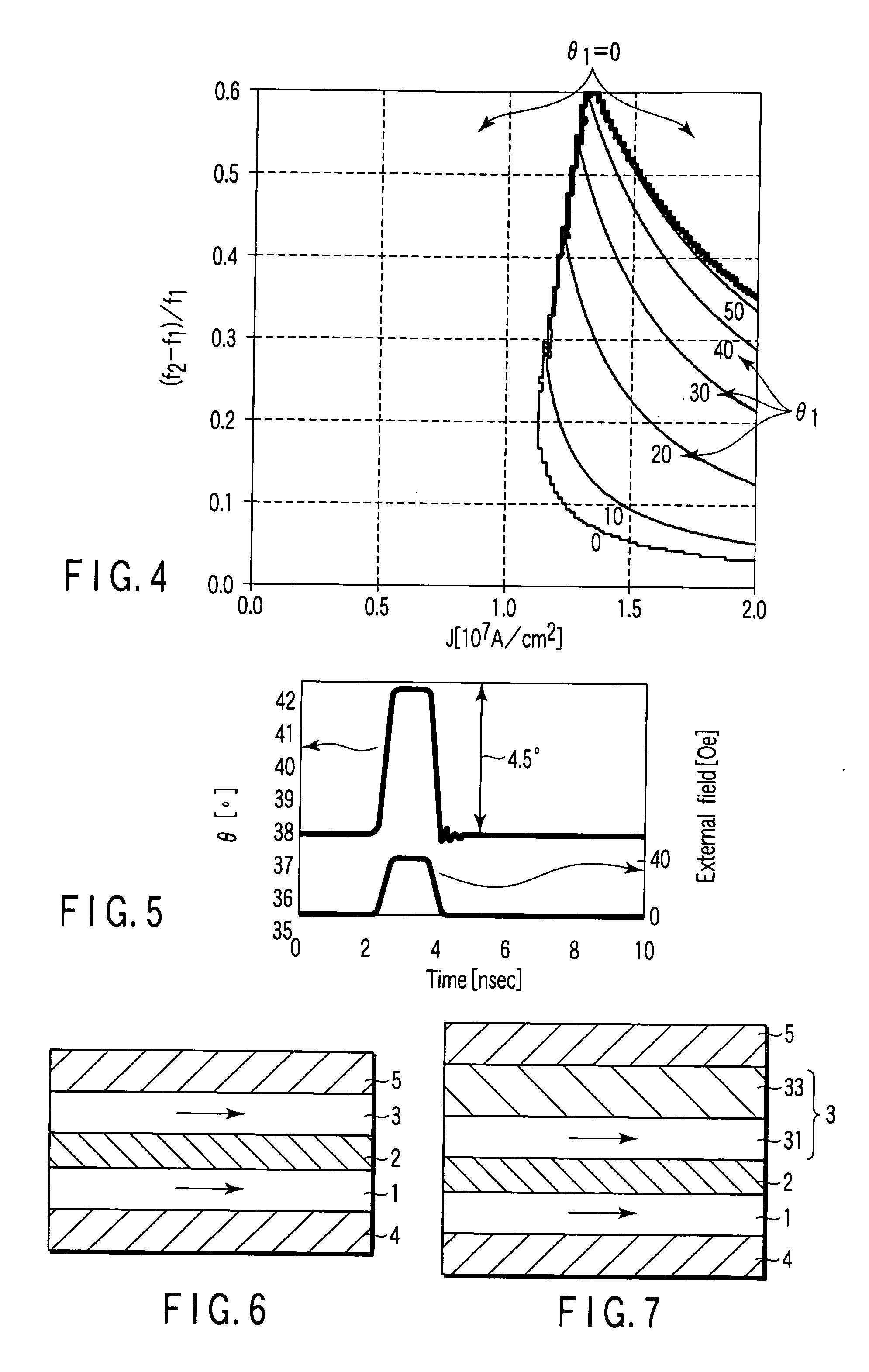
[0114] The magnetic oscillating device in the present example has the structure shown in FIG. 6. Co is used for the first and second magnetic resonance layers 1 and 3. The magnitude of a uniaxial anisotropic field of a Co film is known to vary with the thickness thereof. Thus, Co layers with different film thicknesses are used for the first and second magnetic resonance layers 1 and 3 so as to differentiate the magnetic resonance frequency specific to the first and second magnetic resonance layers 1 and 3. The two Co layers are deposited so as to have magnetic anisotropies in the same direction. Cu is used for the nonmagnetic layer. The deposition is carried out by sputtering.

[0115] First, Cu [100 nm] and Ta [5 nm] are deposited as the lower electrode 4 on a silicon substrate having a thermal oxide film formed thereon. The surface of the lower electrode 4 is polished to improve flatness. On the lower electrode 4, a Co layer with a thickness of about 1.5 nm as the first magnetic res...

example 2

[0117] The magnetic oscillating device in the present example has the structure shown in FIG. 7. The first magnetic resonance layer 1 is formed of a single ferromagnetic layer. The second magnetic resonance layer 3 is formed of an exchange-coupled film in which the ferromagnetic layer 31 and the antiferromagnetic layer 33 are stacked. The present example uses a manufacturing method similar to that in Example 1.

[0118] As shown in FIG. 7, a Cu film with a thickness of 10 nm as the lower electrode 4, a Co film with a thickness of 5 nm as the first magnetic resonance layer 1, a Cu film with a thickness of 3 nm as the nonmagnetic layer 2, a Co film with a thickness of 5 nm as the ferromagnetic layer 31 in the second magnetic resonance layer 3, an IrMn film with a thickness of about 8 nm as the antiferromagnetic layer 33 in the second magnetic resonance layer 3, and a Cu film with a thickness of 10 nm as the upper electrode 5 are used. The device has a junction area of about 100×100 nm2....

example 3

[0120] The magnetic oscillating device in the present example has a structure shown in FIG. 8. The first magnetic resonance layer 1 is formed of an exchange-coupled film in which the ferromagnetic layer 11 and the antiferromagnetic layer 13 are stacked. The second magnetic resonance layer 3 is formed of an exchange-coupled film in which the ferromagnetic layer 31 and the antiferromagnetic layer 33 are stacked. IrMn is used for the antiferromagnetic layers. Co is used for the ferromagnetic layers. The present example uses a manufacturing method similar to that in Example 1.

[0121] Specifically, a Cu layer [about 10 nm], an IrMn layer [about 10 nm], a Co layer [about 3 nm], a Cu layer [about 5 nm], a Co layer [about 3 nm], an IrMn layer [about 7 nm], and a Cu layer [about 20 nm] are stacked. The device has a junction area of about 50×100 nm2.

[0122] In a resonance spectrum through ferromagnetic resonance, peaks corresponding to the exchange-coupled film of the Co layer [about 3 nm] / Ir...


PUM


Abstract

A magnetic oscillating device including a first magnetic resonance layer with a first magnetic resonance frequency f1, a second magnetic resonance layer with a second magnetic resonance frequency f2 higher than the first magnetic resonance frequency f1, a nonmagnetic layer sandwiched between the first magnetic resonance layer and the second magnetic resonance layer, and a pair of electrodes which supplies a current perpendicularly to film planes of the first and second magnetic resonance layers, in which a difference (f2−f1) between the two magnetic resonance frequencies is larger than half a resonance line width of the first magnetic resonance layer, and a ratio of the two magnetic resonance frequencies f2/f1 is 1.6 or less.

Description

CROSS-REFERENCE TO RELATED APPLICATIONS [0001] This application is based upon and claims the benefit of priority from prior Japanese Patent Application No. 2005-103607, filed Mar. 31, 2005, the entire contents of which are incorporated herein by reference. BACKGROUND OF THE INVENTION [0002] 1. Field of the Invention [0003] The present invention relates to a magnetic oscillating device, and a magnetic sensor, a magnetic head, and a magnetic reproducing apparatus using the magnetic oscillating device. [0004] 2. Description of the Related Art [0005] In recent years, a giant magnetoresistive (GMR) element has been commonly used in a magnetic head of a hard disk drive. The spin valve film has a structure in which a magnetization free layer (free layer), a nonmagnetic layer (spacer layer), a magnetization pinned layer (pinned layer), and an antiferromagnetic layer are stacked. In the spin valve film, the magnetization of the pinned layer in fixed by exchange bias with the antiferromagneti...

Claims


Application Information

Patent Timeline
IPC IPC(8): B32B7/02
CPCB82Y25/00G01R33/09G11B5/3903H01F10/3286H01F10/3268H01L43/08Y10T428/24942G11B2005/0002H10N50/10
Inventor KUDO, KIWAMUSATO, RIE
Owner KK TOSHIBA
Why Eureka
Try Eureka