
Method for fabricating semiconductor device

Inactive Publication Date: 2006-10-05
SK HYNIX INC
View PDF7 Cites 5 Cited by
  • Summary
  • Abstract
  • Description
  • Claims
  • Application Information

AI Technical Summary

Benefits of technology

[0025] An embodiment of the invention is a method for fabricating a semiconductor device suitable to control a critical dimension (CD) of a gate line and to prevent an incidence that a landing plug contact hole is not properly opened.

Problems solved by technology

Accordingly, there are a lot of difficulties in fabricating such semiconductor devices.
Particularly, through an etching process and a lithography process, damage such as evaporation of the metal layer may be generated.
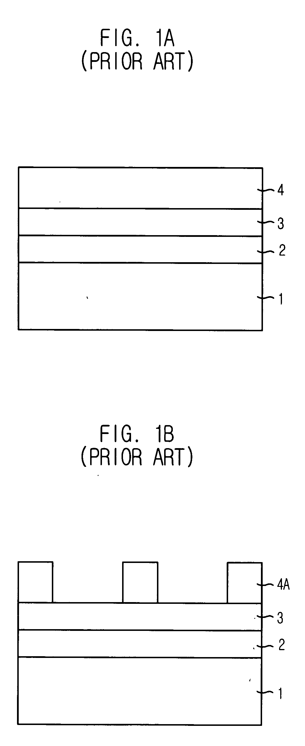
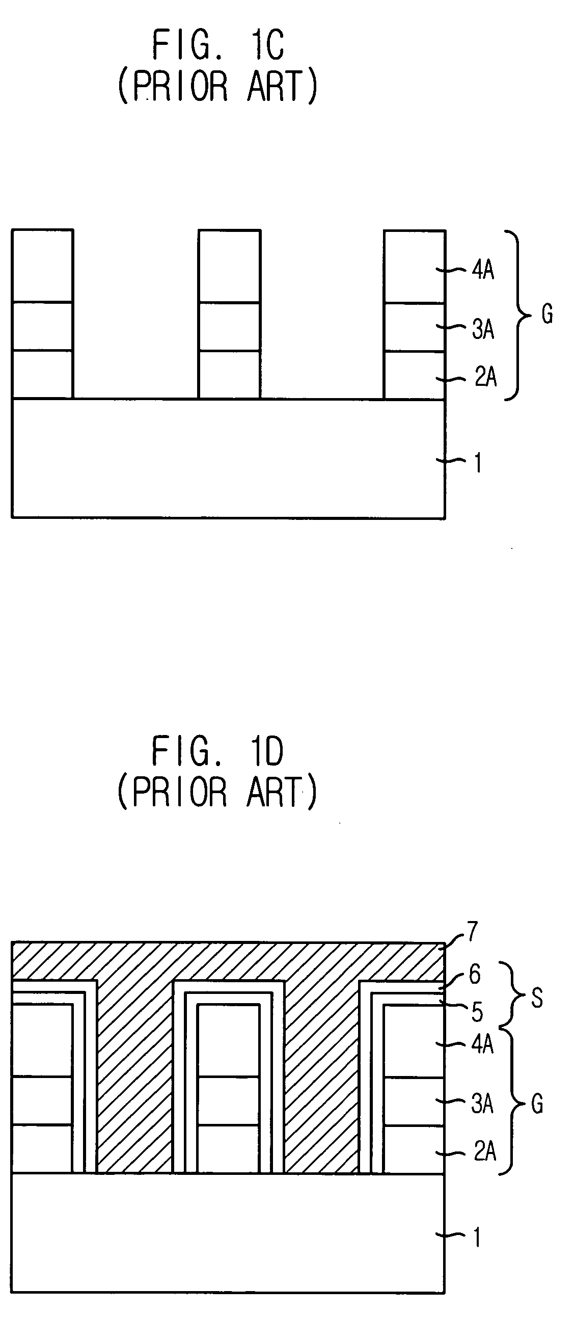
Accordingly, as a distance between the unit devices of the DRAM device is decreased and a height of a gate line is increased, the gate line formation reaches a limitation and LPC formation also faces a difficulty.
That is, during forming the gate lines, it may be difficult to control critical dimensions of the gate lines, and yields of products may be decreased, due to damage in the gate lines and a contact hole not-open event.

Method used


Image

  • Method for fabricating semiconductor device
  • Method for fabricating semiconductor device
  • Method for fabricating semiconductor device

Examples


Embodiment Construction

[0030] Hereinafter, detailed descriptions on certain embodiments of the present invention will be provided with reference to the accompanying drawings.

[0031]FIGS. 2A to 2H are cross-sectional views illustrating a method for fabricating a semiconductor device in accordance with an embodiment of the present invention.

[0032] As shown in FIG. 2A, an isolation process is performed in a substrate 21, thereby forming a device isolation layer (not shown).

[0033] Next, a gate oxidation is performed, thereby forming a gate oxide layer (not shown) on the substrate 21.

[0034] Next, a gate conductive layer 22 is formed on the gate oxide layer (not shown). At this time, the gate conductive layer 22 uses a polysilicon layer. A plurality of photoresist patterns 23 are formed on the gate conductive layer 22.

[0035] As shown in FIG. 2B, the gate conductive layer 22 and the gate oxide layer (not shown) are patterned by using the photoresist patterns 23 as an etch mask. Herein, a reference numeral 22...


PUM


Abstract

First gate lines are formed on a substrate. An insulation layer is formed on the substrate and the first gate lines. The insulation layer disposed between the first gate lines is selectively etched, to thereby form first openings. Landing plugs are buried into the first openings. The insulation layer disposed on the first gate lines is etched until upper portions of the first gate lines are exposed, thereby obtaining second openings. Second gate lines are formed inside the second openings.

Description

FIELD OF THE INVENTION [0001] An embodiment of the present invention relates to a method for fabricating a semiconductor device; and more particularly, to a method for fabricating a gate line and a landing contact plug using a damascene process. DESCRIPTION OF RELATED ARTS [0002] Typically, semiconductor devices include a plurality of unit devices. As the semiconductor devices have been highly integrated, the unit devices should be formed with a high density on a fixed cell area. Accordingly, the sizes of the unit devices, i.e., transistors and capacitors, have been decreased. Particularly, in the semiconductor devices such as dynamic random access memory (DRAM) devices, as a design rule has been decreased, the sizes of the semiconductor devices formed inside of the cell have also been decreased. Recently, the semiconductor device has a minimum line width of less than 0.1 μm. Even a line width size of less than 80 nm is needed. Accordingly, there are a lot of difficulties in fabrica...

Claims


Application Information

Patent Timeline
IPC IPC(8): H01L21/44
CPCH01L21/76897H01L27/10888H01L27/10855H10B12/485H10B12/0335A47J31/085A47J31/46A47J31/58A47J31/4403
Inventor SEO, DAE-YOUNG
Owner SK HYNIX INC
Learn More