
Full fault tolerant architecture for organic electronic devices

a technology of electronic devices and fault tolerance, applied in static indicating devices, instruments, electroluminescent light sources, etc., can solve the problems of shorting between the anode and the cathode of the oled, high production and commercial expenses of lcd displays, and high cost of developmen

Inactive Publication Date: 2006-10-12
GENERAL ELECTRIC CO
View PDF11 Cites 14 Cited by
  • Summary
  • Abstract
  • Description
  • Claims
  • Application Information

AI Technical Summary

Problems solved by technology

However, the LCD displays involve high production and commercial expenses.
However, the development of large area OLEDs is difficult due to failures of the OLED devices owing to the presence of local defects that cause electrical shorts and electrical opens.
Typically, particle contamination during fabrication, asperities from electrode roughness and non-uniformities in organic layer thickness may cause shorting between the anode and cathode of the OLED.
Also, a loss of electrical connectivity in an OLED may cause an electrical open.

Method used


Image

  • Full fault tolerant architecture for organic electronic devices
  • Full fault tolerant architecture for organic electronic devices
  • Full fault tolerant architecture for organic electronic devices

Examples


exemplary embodiment 100

[0048] Referring to FIG. 10, a second exemplary embodiment 100 of an organic device package is illustrated. In a presently contemplated configuration, the organic device package 100 is illustrated diagrammatically as having a plurality of modules of organic electronic elements. In the exemplified embodiment, the organic device package 100 is depicted as including a first module 102, a second module 104, and a third module 106 of organic electronic elements. However, as will be appreciated by one skilled in the art, in alternate embodiments of the present technique, a lesser or greater number of modules of organic electronic elements may be envisaged. The modules 102, 104, 106 of organic electronic elements may be electrically connected in a series arrangement to form the organic device package 100. Further, the first and second modules 102, 104 may be electrically coupled in series via a series interconnection area 108. Likewise, the second and third modules 104, 106 may be arranged...

exemplary embodiment 120

[0056] Turning to FIG. 11 an exemplary embodiment 120 of the organic device package 10 of FIG. 1 is illustrated. In this embodiment, the organic device package 120 may be formed by arranging a plurality of organic electronic elements between a plurality of nodes. As used herein, a “node” is used to represent a connection point between organic electronic elements. Also, each of the plurality of organic electronic elements may include an organic electronic device.

[0057] In a presently contemplated configuration, a first organic electronic element 122 may be coupled between a first node 124 and a second node 126. Similarly, a second organic electronic element 128 may be coupled between the second node 126 and a third node 130. Consequent to coupling the first organic electronic element 122 between the first and second nodes 124, 126 and coupling the second organic electronic element 128 between the second and third nodes 126, 130, a first sub-group 132 of organic electronic elements ma...


PUM


Abstract

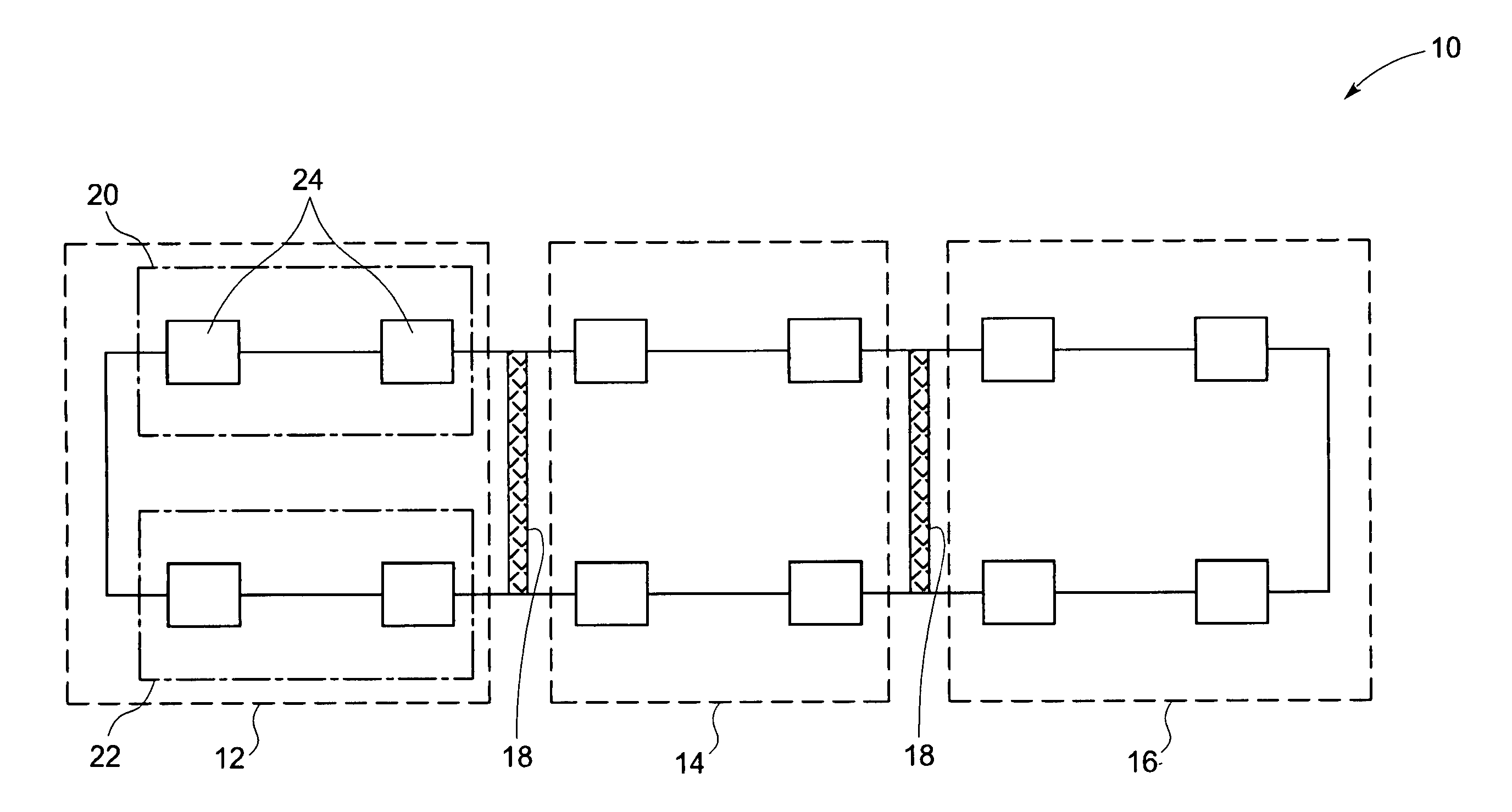
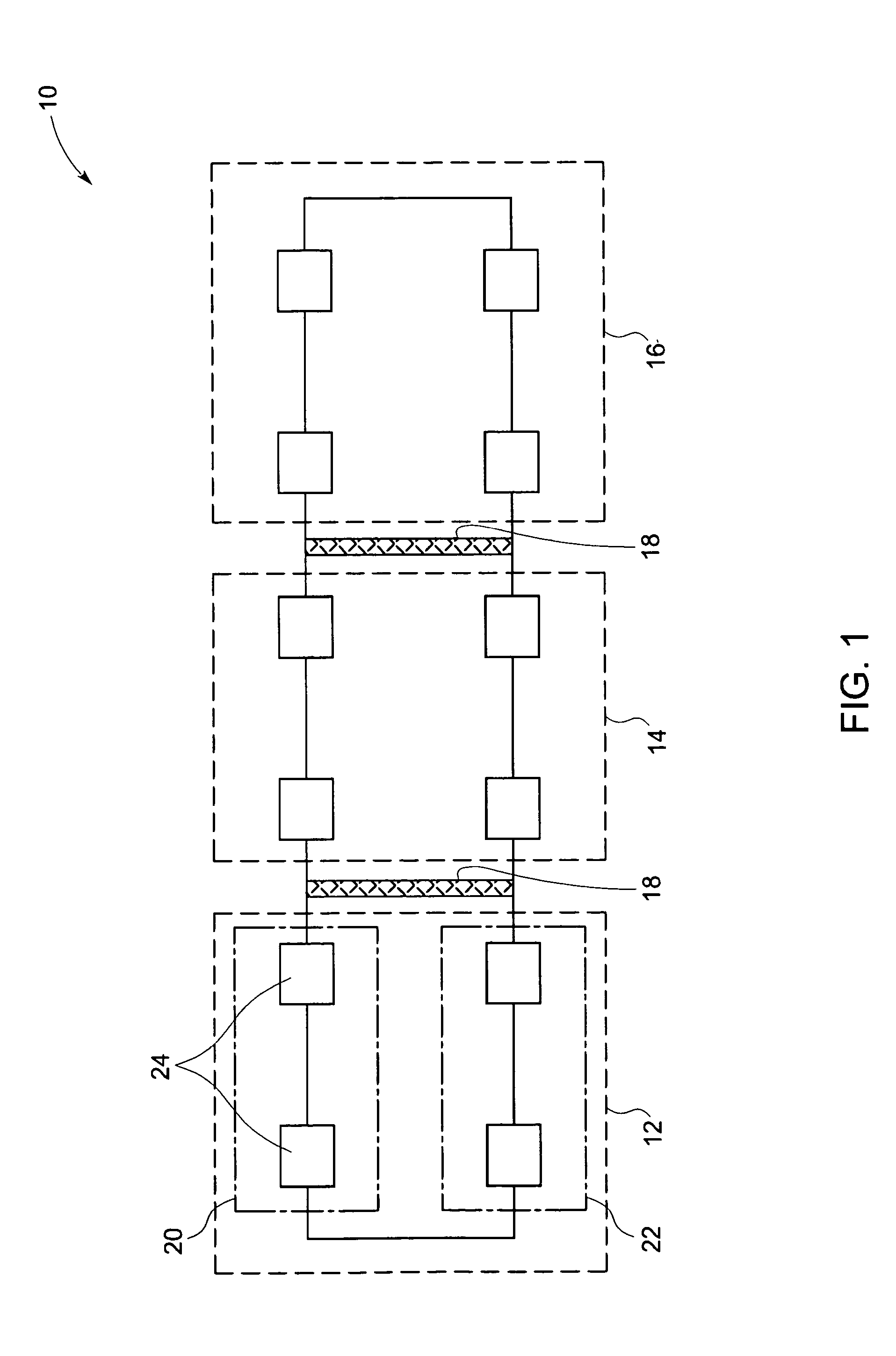
An organic device package that provides full fault tolerance against both electrical shorts and electrical opens is presented. An organic device package comprising a plurality of groups of organic electronic elements electrically coupled in series, where at least one of the plurality of groups of organic electronic elements comprises a plurality of sub-groups of organic electronic elements electrically coupled in parallel, and where at least one of the plurality of sub-groups of organic electronic elements comprises a plurality of organic electronic elements electrically coupled in series. Further, various embodiments are contemplated where a plurality of series blocks and parallel blocks may be nested to provide a grid network having increased flexibility and fault tolerance.

Description

STATEMENT REGARDING FEDERALLY SPONSORED RESEARCH & DEVELOPMENT [0001] This invention was made with Government support under contract number 70NANB3H3030 awarded by National Institute of Standards and Technology. The Government has certain rights in the invention.BACKGROUND [0002] The invention relates generally to lighting devices, and more particularly to organic electronic devices. [0003] Currently, organic electronic devices, such as, but not limited to, organic light emitting diodes (OLEDs), are being increasingly employed for display applications and for lighting applications. In the last decade, tremendous progress has been made in the area of OLEDs. Previously, liquid crystal displays (LCDs) were employed for most display applications. However, the LCD displays involve high production and commercial expenses. [0004] With the imaging appliance revolution underway, the need for more advanced devices that provide advanced display and / or lighting features is increasing. Further, ...

Claims


Application Information

Patent Timeline
IPC IPC(8): H01L23/02H05B44/00
CPCG09G3/006G09G3/3208H01L51/5203H01L27/3202H01L27/3204G09G2330/08H10K59/84H10K59/86H10K59/82H10K50/805
Inventor LIU, JIEDUGGAL, ANIL RAJ
Owner GENERAL ELECTRIC CO
Learn More