Level shifter circuit

Inactive Publication Date: 2006-10-12
RENESAS ELECTRONICS CORP
View PDF6 Cites 7 Cited by
  • Summary
  • Abstract
  • Description
  • Claims
  • Application Information

AI Technical Summary

Benefits of technology

[0015] According to the present invention, it is possible to form a level shifter circuit with a higher operating speed than that of the conventional level shifter circuits. Furthermore, when the voltage (second power supply voltage V2 in an embodiment) of the high voltage side

Problems solved by technology

In the level shifter shown in FIG. 1, as described above, a plurality of steps are necessary for the change from Low level to High level, and thus high-speed operation may be difficult.
In a case when an input signal of power supply voltage lower than the power supply vo

Method used


Image

  • Level shifter circuit
  • Level shifter circuit
  • Level shifter circuit

Examples


Example

First Embodiment

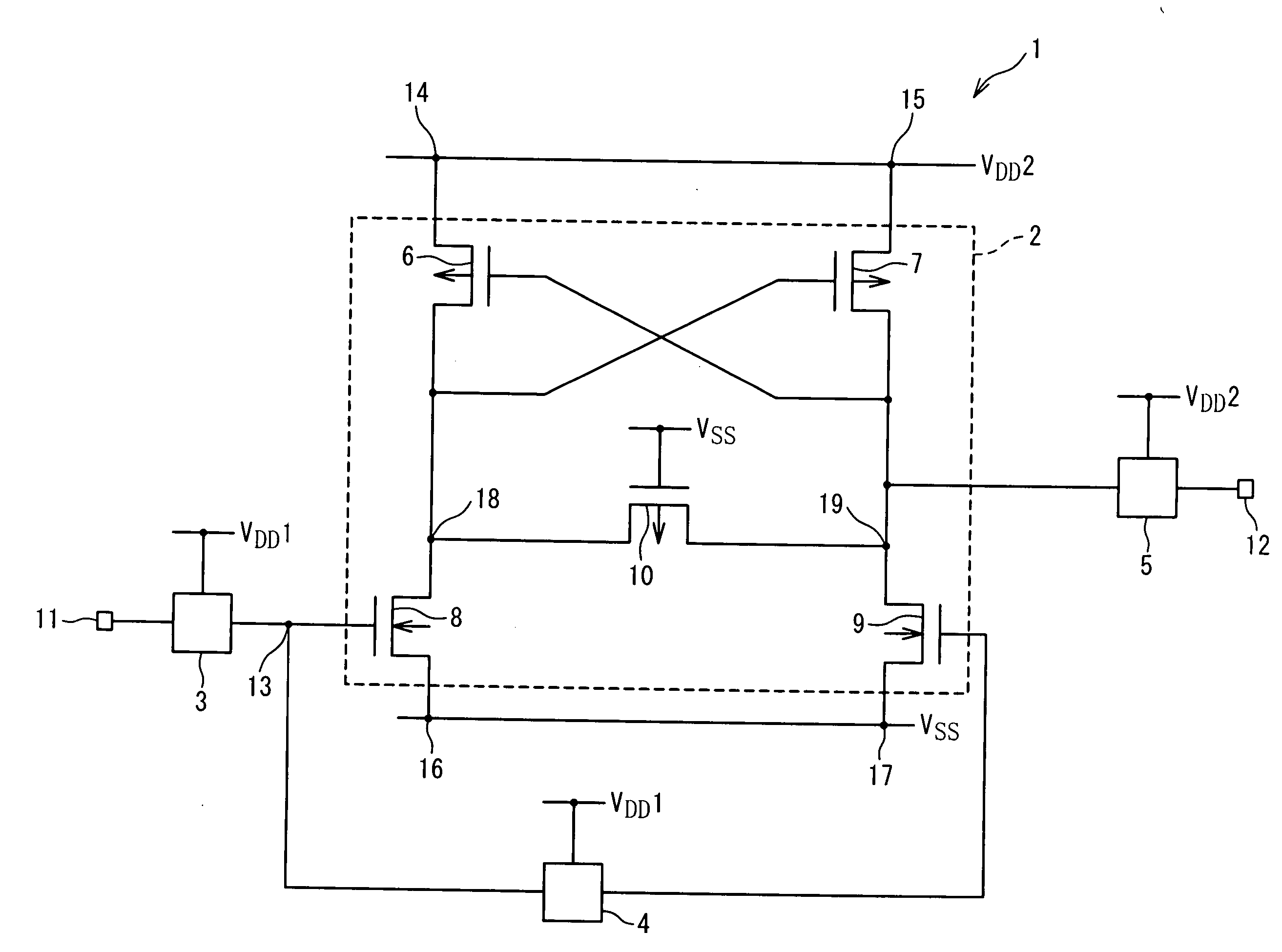
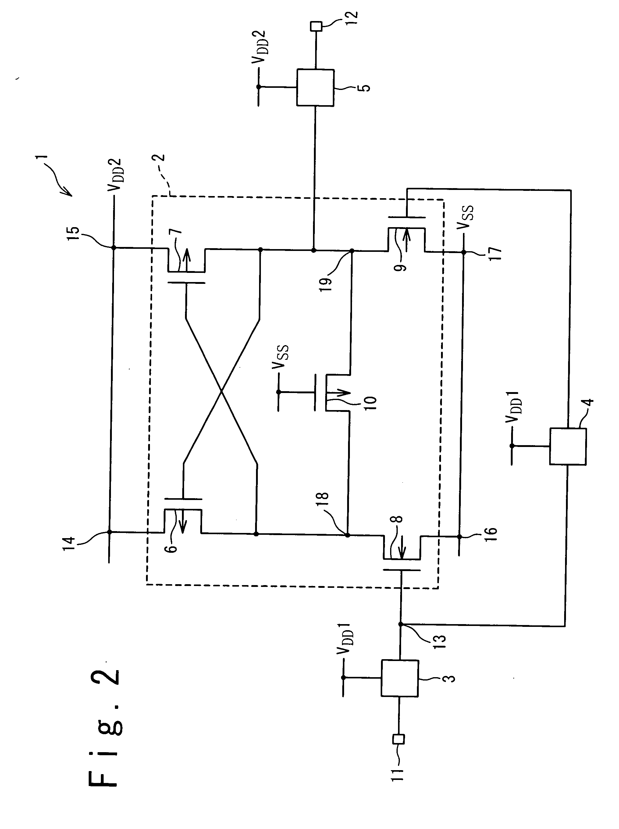
[0036]FIG. 2 is a circuit diagram showing a configuration of a level shifter circuit 1 according to a first embodiment. In the present embodiment, a first power supply voltage V1 is supplied from a first power supply line VDD1, and a second power supply voltage V2 is supplied from a second power supply line VDD2. Here, the first power supply voltage V1 is smaller than the second power supply voltage V2.

[0037] Referring to FIG. 2, the level shifter circuit 1 according to the present embodiment includes a level shifter part 2, a first logic circuit 3, a second logic circuit 4 and a first output logic circuit 5. The first logic circuit 3 is a logic circuit for generating a first input signal in response to a basic input signal supplied through an input terminal 11. The first input signal output from the first logic circuit 3 is supplied to a first NMOS transistor 8 of the level shifter part 2 via a first node 13. The first input signal is also input to the second logi...

Example

Second Embodiment

[0057]FIG. 9 is a circuit diagram showing a configuration of a level shifter circuit 1 according to a second embodiment of the present invention. Referring to FIG. 9, the level shifter part 2 in the second embodiment has a passive resistive element 21 which is connected between the sixth node 18 and the seventh node 19. The level shifter circuit 1 in the above-mentioned first embodiment is provided with the MOS transistor between the sixth node 18 and the seventh node 19 as the resistive element. As shown in FIG. 9, the level shifter circuit 1 according to the second embodiment has the passive resistive element 21 as the resistive element. The passive resistive element 21 is a resistance element having the same resistance as the ON resistance of the foregoing resistive element 10 (or the resistance NMOS transistor 20). Such the passive resistive element 21 is connected between the sixth node 18 and the seventh node 19. As a result, the passive resistive element 21 ...

Example

Third Embodiment

[0058]FIG. 10 is a circuit diagram showing a configuration of a level shifter circuit 1 according to a third embodiment of the present invention. Referring to FIG. 10, the level shifter part 2 in the third embodiment has a resistance MOS transistor 22 which is connected between the sixth node 18 and the seventh node 19. As shown in FIG. 10, a gate of the resistance MOS transistor 22 is connected to a power down signal input terminal 23. Supplied to the level shifter part 2 through the power down signal input terminal 23 is a power down signal PD which can deactivate the resistance MOS transistor 22. That is, the resistance MOS transistor 22 can be set to an OFF state by the power down signal PD. The resistance MOS transistor 22 shown in FIG. 10 is a PMOS transistor. It is therefore possible to deactivate the resistance PMOS transistor 22 by applying the second power supply voltage V2 as the power down signal PD, for example. According to the configuration, as descri...


PUM


Abstract

A level shifter circuit has first to fourth transistors and a resistive element. The first transistor is activated in response to a logic signal whose high level voltage is a first voltage. The second transistor is activated in response to the inverse logic signal. Each of the first and second transistors is connected between a power supply line for supplying a second voltage and a ground line. The third transistor is connected to a drain of the first transistor through a first node. The fourth transistor is connected to a drain of the second transistor through a second node. A gate of the third transistor is connected to the drain of the second transistor through the second node. A gate of the fourth transistor is connected to the drain of the first transistor through the first node. The resistive element is connected between the first node and the second node.

Description

BACKGROUND OF THE INVENTION [0001] 1. Field of the Invention [0002] The present invention relates to a level shifter circuit. [0003] 2. Description of the Related Art [0004] When circuits operating with different power supply voltages are connected to each other, a level shifter circuit has been widely used and provided between the circuits. The level shifter circuit shifts the level of power supply voltage to ensure consistency. The level shifter circuit shifts up (or shifts down) the signal level of a former circuit so as to correspond to the signal level of a latter circuit side, and supplies the shifted-up (shifted-down) signal to the latter circuit. [0005] For example, let us consider a case where a circuit operating with a low power supply voltage is connected to a circuit operating with a high power supply voltage. In this case, a level shifter circuit shifts up a signal from the low power supply voltage operating circuit side to a signal of the high power supply voltage leve...

Claims


Application Information

Patent Timeline
IPC IPC(8): H03K19/0175
CPCH03K3/356182
Inventor SHIMAYA, HIROSHI
Owner RENESAS ELECTRONICS CORP
Why Eureka
Try Eureka