Liquid crystal display and method of manufacturing the same

a liquid crystal display and liquid crystal technology, applied in the field of liquid crystal display, can solve the problems of affecting the original liquid crystal alignment, difficult to restore the initial state of singular points, and difficulty in controlling the alignment of liquid crystal molecules with the electrode units, etc., to achieve stable liquid crystal alignment, high display quality, and simplified process

Inactive Publication Date: 2006-10-12
SHARP KK
View PDF8 Cites 6 Cited by
  • Summary
  • Abstract
  • Description
  • Claims
  • Application Information

AI Technical Summary

Benefits of technology

[0016] In this case, the metal light shield film is formed using photolithography and etching, and the photo-resist used for patterning the film is baked and left on the metal light shield film to adjust the height of the surface of the common electrode, whereby the process can be simplified.
[0017] It is expected that the same advantage can be achieved by forming color separation filter layers in different colors one after another on the metal light shield film.
[0018] According to the invention, since the surface of the common electrode facing the non-electrode part at the outer periphery of the electrode unit is at a height of 0.2 μm or more or at a height in the range from 0.4 to 1.5 μm if possible above the height of the surface of the common electrode facing the part of the electrode unit substantially in the middle thereof, electric fields at the outer periphery of the electrode unit have a strong force of regulating liquid crystal alignment. Thus, more stable liquid crystal alignment is achieved, and any disturbance of alignment attributable to an external force can be corrected to provide a liquid crystal display having high display quality and stability.
[0019] A step can be formed on the common electrode without any unnecessary pattern protruding into a transmissive part by forming the photo-resist and the color separation filter layer in the order listed on the metal light shield film or forming the color separation filter layers in different colors one after another on the metal light shield film. It is therefore possible to provide a low-cost and high quality liquid crystal display without any additional process for forming the step.
[0020] Further, since the metal light shield film is formed using photolithography and etching, and the photo-resist used for patterning is baked and left on the metal light shield film, the height of the surface of the common electrode can be adjusted in an ideal position, which makes it possible to provide a liquid crystal display of high accuracy and high quality without any additional process.

Problems solved by technology

However, since the electrode units themselves of the liquid crystal display in the example are entirely composed of solid patterns as shown in FIG. 27, there will be a large area in which the alignment of liquid crystal molecules can not be controlled with the electrode units when the patterns are large.
When an external force is applied to the panel of the liquid crystal display by a press with a finger, it is difficult to restore the initial state of singular points which are thus once disturbed.
Further, when edges of the electrode units are close to gate bus lines or drain bus lines, the original liquid crystal alignment is affected by electric fields generated between the edges and the bus lines.
In the structure disclosed in the specification, since a surface of a common electrode on a CF substrate facing a central part of a pixel electrode unit is at the same height as a surface of the common electrode of the CF substrate facing a non-electrode part at the outer periphery of the electrode unit, there is no measure for fixing singular points of liquid crystal alignment outside the electrode unit, which results in a problem that there is a large area in which the alignment of liquid crystal molecules cannot be controlled.
As thus described, difficulty in controlling singular points increases when the size of an electrode unit is increased.

Method used


Image

  • Liquid crystal display and method of manufacturing the same
  • Liquid crystal display and method of manufacturing the same
  • Liquid crystal display and method of manufacturing the same

Examples


first embodiment

[0048] A liquid crystal display and a method of manufacturing the same according to a first embodiment of the invention will now be described with reference to FIGS. 1 to 11.

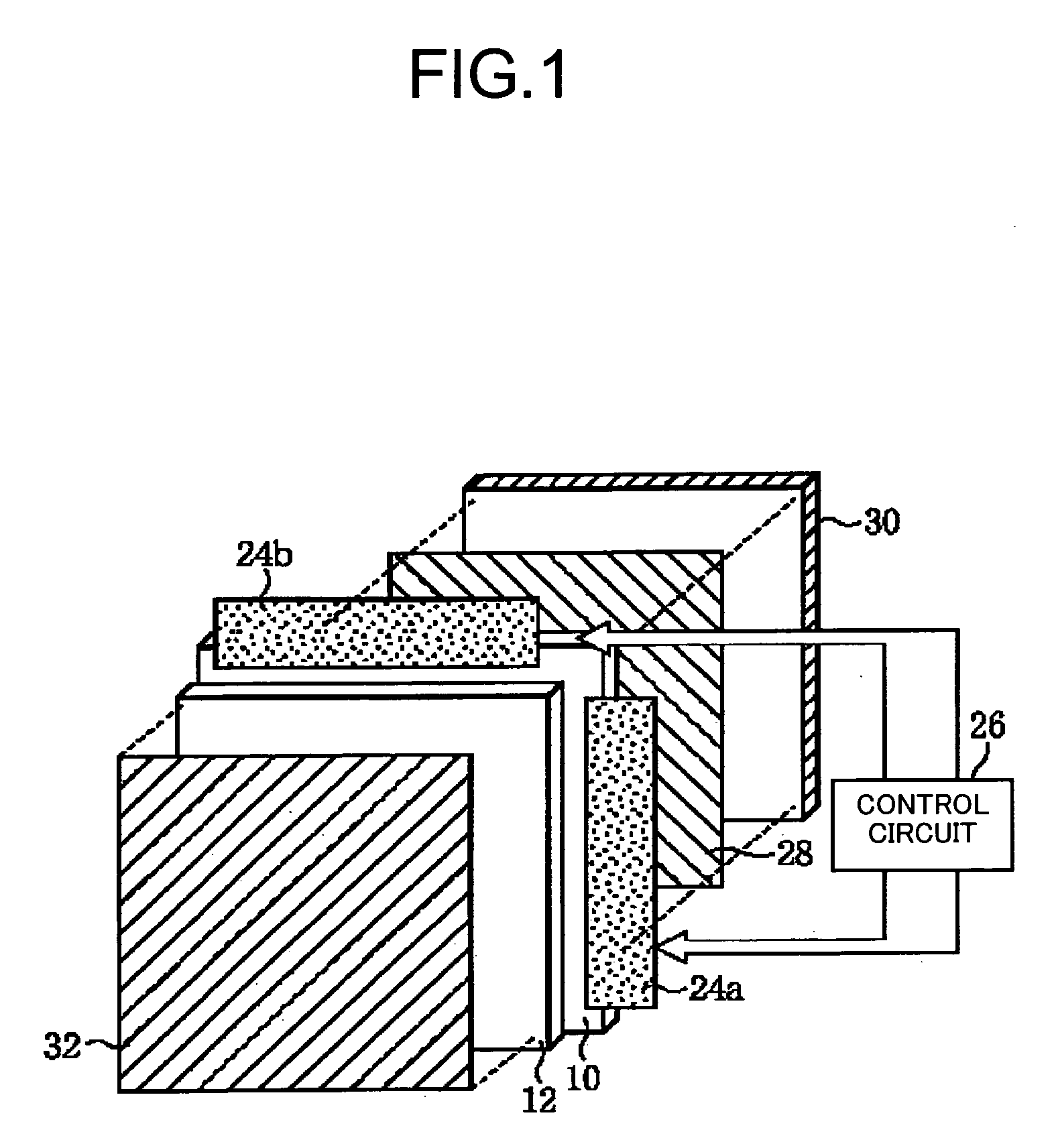
[0049] As shown in FIG. 1, the liquid crystal display of the present embodiment has a structure in which a TFT substrate 10 having TFT (thin film transistors) formed thereon and a CF substrate 12 having CFs (color filters) formed thereon are combined in a face-to-face relationship and in which a liquid crystal is sealed between the substrates 10 and 12.

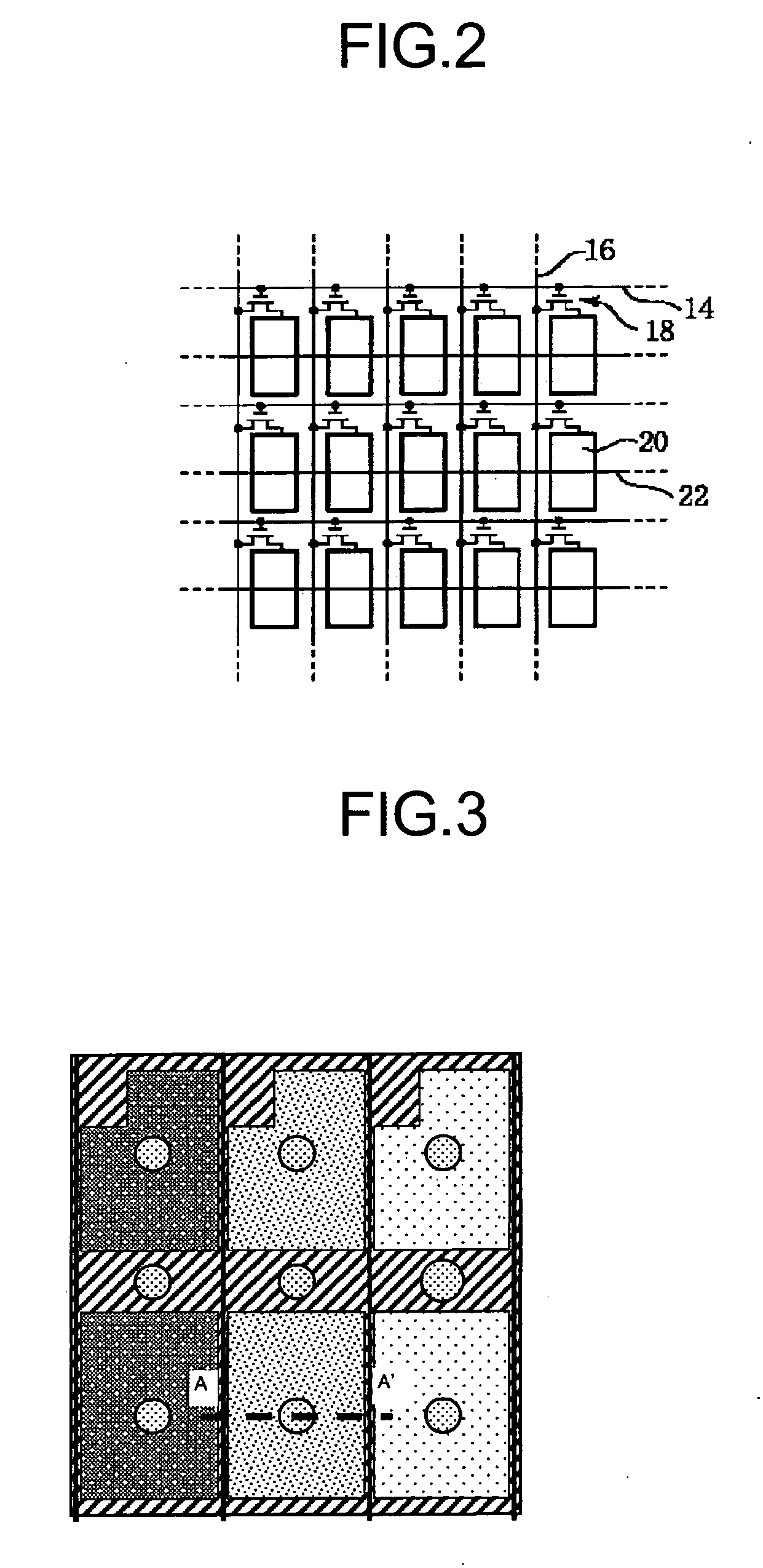
[0050]FIG. 2 schematically shows an equivalent circuit of elements formed on the TFT substrate 10. A plurality of gate bus lines extending in the horizontal direction in the figure are formed in parallel with each other on the TFT substrate 10. A plurality of drain bus lines 16 extending in the vertical direction in the figure are formed in parallel with each other so as to intersect with the gate bus lines 14 with an insulation film interposed between them. Eac...

second embodiment

[0064] A liquid crystal display and a method of manufacturing the same according to a second embodiment of the invention will now be described with reference to FIGS. 12 to 17. A TFT substrate and a CF substrate in the present embodiment are identical in structure to those in the first embodiment. However, the method of manufacturing a BM layer on a CF substrate is different from the first embodiment. The method of manufacturing a CF substrate in the present embodiment will be described with reference to FIGS. 12 to 17.

[0065] A film of a light shield metal 101 such as chromium is formed on a transparent insulation substrate 60 such as a glass, and a positive resist is applied to the substrate to a thickness of 1.5 μm. After drying the applied film at a temperature of about 100° C., a desired BM pattern 102 is exposed with an exposure energy of about 70 mJ using a proximity aligner. The substrate is then shower-developed using a TMAH developer at an alkali concentration of 2.38% and...

third embodiment

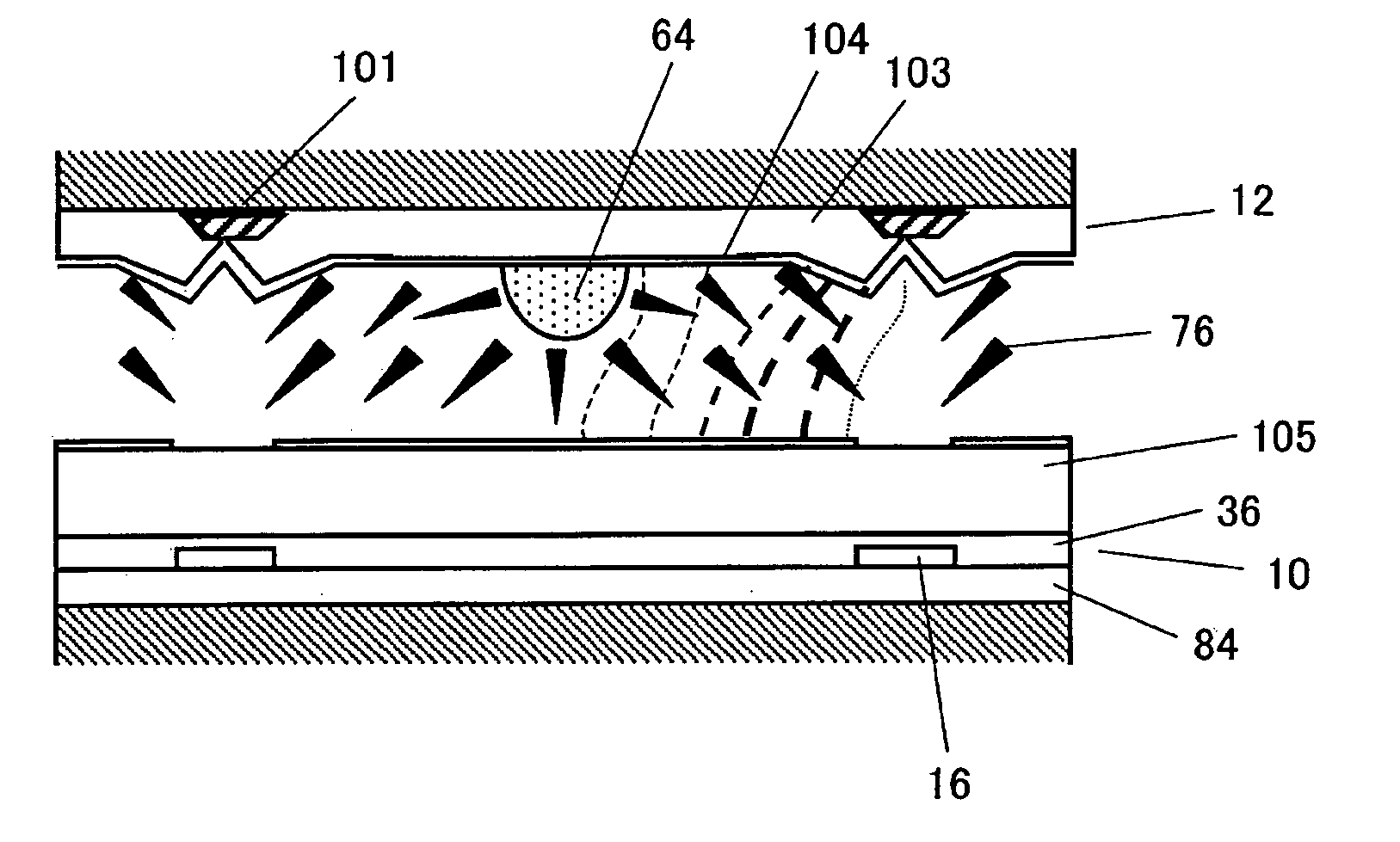
[0071] A liquid crystal display and a method of manufacturing the same according to a third embodiment of the invention will now be described with reference to FIGS. 18 to 24. FIG. 18 is a sectional view of the liquid crystal display of the present embodiment. Just like the first embodiment, the display has a structure in which a TFT substrate and a CF substrate are combined in a face-to-face relationship and a liquid crystal is sealed between the substrate. The TFT substrate has the same structure as that in the first embodiment. The CF substrate has a structure as follows. Color separation filters in different colors are formed one after another on a BM layer constituted by a metal light shield film formed on a transparent insulation substrate such as a glass, so that steps on the surface of a common electrode above light shield regions at drain wiring portions and storage capacitor portions are adjusted to have a height in the range from 0.4 to 0.6 μm.

[0072] A method of fabricat...


PUM

PropertyMeasurementUnit
heightaaaaaaaaaa
heightaaaaaaaaaa
widthsaaaaaaaaaa

Abstract

The invention relates to a vertically aligned liquid crystal display and a method of manufacturing the same and provides a liquid crystal display in which singular points can be sufficiently controlled to achieve high display quality and a method of manufacturing the same. A liquid crystal display includes a first substrate having a pixel electrode including one or more electrode units electrically connected to each other, a second substrate facing the pixel and having a light shield portion constituted by a metal film, a color separation filter at an opening thereof, and a common electrode on a surface thereof, and a liquid crystal layer having negative dielectric constant anisotropy sealed between the first substrate and the second substrate. A surface of the common electrode facing at least one-fourth of a non-electrode part at the outer periphery of the electrode unit is formed with a height of 0.2 μm or more or a height in the range from 0.4 to 1.5 μm if possible above a surface of the common electrode facing a part of the electrode unit substantially in the middle thereof.

Description

BACKGROUND OF THE INVENTION [0001] 1. Field of the Invention [0002] The present invention relates to a liquid crystal display and a method of manufacturing the same and, more particularly, to a vertically aligned liquid crystal display and a method of manufacturing the same. [0003] 2. Description of the Related Art [0004] In a vertically aligned liquid crystal display, a liquid crystal having negative dielectric constant anisotropy is vertically aligned using vertical alignment films when no voltage is applied and aligned at a tilt when a voltage is applied. Since liquid crystal molecules are vertically aligned when no voltage is applied, a vertically aligned liquid crystal display has advantages including high quality in displaying black, and capability of displaying at a high contrast, a wide viewing angle, and high response. [0005] For example, methods of regulating the alignment of the liquid crystal of such a vertically aligned liquid crystal display include a pixel configurati...

Claims


Application Information

Patent Timeline
Patent Type & Authority Applications(United States)
IPC IPC(8): G02F1/1337
CPCG02F1/133707G02F2201/121G02F1/1393G02F1/1335
Inventor SAWASAKI, MANABUTAKAGI, TAKASHI
Owner SHARP KK
Why Eureka
Try Eureka