Organic optoelectronic device

a technology of optoelectronic devices and optical contacts, which is applied in the direction of solid-state devices, semiconductor devices, electrical apparatus, etc., can solve the problems of difficult connection in this manner, difficult to connect driving electronics to the edge of the substrate, and complex routing of electrical contacts, etc., to achieve better appearance, less black spots, and longer life

Inactive Publication Date: 2006-10-19
CAMBRIDGE DISPLAY TECH LTD
View PDF10 Cites 39 Cited by
  • Summary
  • Abstract
  • Description
  • Claims
  • Application Information

AI Technical Summary

Benefits of technology

[0019] In the organic optoelectronic devices of the present invention light enters or leaves the device through the cathode which is transparent or semi-transparent. Where the organic optoelectronic device is an organic electroluminescent device this type of device is known as a top emitter. The device architecture provided by the present invention has the advantage over devices of the prior art in that the cathode does not come into contact with the deleterious material used to fill the vias or to bond the conductive vias to the electroluminescent device. In the devices of the prior art emission occurs through the transparent anode so to avoid interfering with the light emission from the display the vias must contact the other side of the diode i.e. the sensitive material of the cathode.
[0020] The inventors of the present invention have solved the problem of deterioration of the cathode material and thereby provided an organic optoelectronic device having a longer lifetime and better appearance, in particular with fewer black s

Problems solved by technology

The disadvantage of this method is that where more complex arrangements of organic diodes are required, as is the case in display applications, the routing of the electrical contacts becomes complex and in particular the attachment of driving electronics to the edge of the substrate may become problematic.
As passive matrix displays on a single monolithic substrate require contacts to be made to the edge of the substrate displays of this type are difficult to connect in this manner without the seams between neighbouring substrates being visible in the eventual display.
But such active matrix displays are very complex and expensive to prepare.
Moreover the low yield of the process used to

Method used


Image

  • Organic optoelectronic device
  • Organic optoelectronic device
  • Organic optoelectronic device

Examples


Embodiment Construction

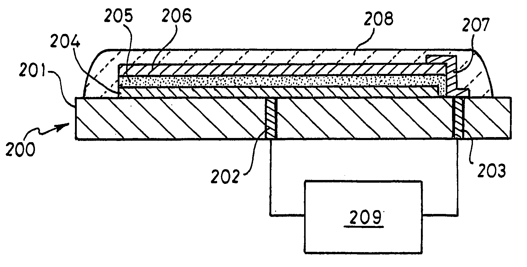
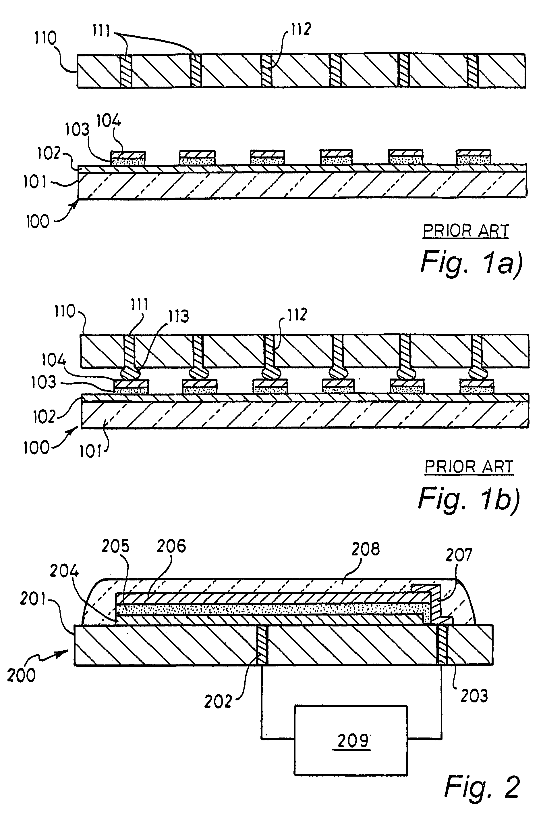
[0064] An optoelectronic device according to the present invention is shown in FIG. 2. The optoelectronic device 200 comprises a substrate 201 through which connecting vias 202203 have been provided. Over the upper surface of the substrate 201 and in electrical contact with via 202 lies a layer of anode material 204. The anode is in turn covered by a layer of organic optoelectronic material 205 over which lies the cathode 206. An electrical connector 207 serves to connect the cathode 206 to via 203. The organic diode is encapsulated with a layer of passivating material 208 and the anode and cathode are connected to driving circuitry 209.

[0065] The substrate may be rigid or flexible and is generally opaque although in some cases a transparent or semi-transparent substrate may be used.

[0066] The substrate typically comprises a material selected from the group comprising ceramics and plastics. The term ceramic is taken to include both ceramics and glasses. Ceramics include high tempe...


PUM

PropertyMeasurementUnit
Electrical conductoraaaaaaaaaa
Transparencyaaaaaaaaaa
Semiconductor propertiesaaaaaaaaaa

Abstract

An organic optoelectronic device includes a substrate having an upper surface and a lower surface, at least one organic diode situated on the upper surface of the substrate, the organic diode including, an anode including a material of high work function situated over the upper surface of the substrate, an organic optoelectronic material at least partially overlaying the anode, a cathode including a material of low work function at least partially overlaying the organic optoelectronic material, the cathode being transparent or semi-transparent, wherein the substrate includes at least one connecting via extending through the substrate from the lower surface to the upper surface, the connecting via being suitable for providing an electrical connection between at least one of the anode and/or the cathode of the organic diode and an external circuit. The invention has application in organic light emitting devices and organic photovoltaic devices.

Description

BACKGROUND OF THE INVENTION [0001] 1. Field of the Invention [0002] The present invention relates to an organic optoelectronic device, a display device comprising said organic optoelectronic device and a method of preparing said organic optoelectronic device. [0003] 2. Brief Description of the Prior Art [0004] The past decade has seen an increasing amount of research into the use of organic materials in optoelectronic devices, examples of such devices include organic electroluminescent devices, as disclosed in WO90 / 13148 and organic photovoltaic devices, as disclosed in U.S. Pat. No. 5,670,791. Both organic electroluminescent devices and organic photovoltaic devices are organic diodes comprising a layer of organic material between two electrodes. Organic electroluminescent devices emit light on the passage of a current between the two electrodes. Organic photovoltaic devices generate a current between the two electrodes when light is incident upon the device. [0005] To provide curre...

Claims


Application Information

Patent Timeline
IPC IPC(8): H01L33/00H01L27/15H01L27/32H01L51/00H01L51/30H01L51/52
CPCH01L27/3288H01L27/3293H01L51/0036H01L51/0037H01L51/5234H01L51/0039H01L51/0059H01L51/007H01L51/0081H01L51/0038H10K59/179H10K59/18H10K85/114H10K85/113H10K85/115H10K85/1135H10K85/631H10K85/6565H10K85/324H10K59/80524H10K50/828
Inventor CARTER, JULIAN
Owner CAMBRIDGE DISPLAY TECH LTD
Why Eureka
Try Eureka