Liquid crystal display device and method for manufacturing the same

Active Publication Date: 2006-10-19
NEC LCD TECH CORP
View PDF1 Cites 35 Cited by
  • Summary
  • Abstract
  • Description
  • Claims
  • Application Information

AI Technical Summary

Benefits of technology

[0033] According to the fifth and sixth aspects of the present invention, since an alignment film is printed on the surface of the first substrate using an alignment plate that has a cut-out part formed in the end part, an alignment film in which a cut-out part is formed in the end part can be formed without increasing the number of steps. Furthermore, since a cut-out part is formed in the end part of the alignment film, the thick film region formed in the end part of the alignment film can b

Problems solved by technology

However, the following problems have been encountered in the abovementioned prior art.
Specifically, the following problem arises in the case of methods in which electrical conductivity of the upper and lower substrates is obtained by piercing the alignment films by means of conductive particles as in the liquid crystal display devices of Japanese Laid-Open Patent Application Nos. 2001-183690 and 11-2820.
Namely, a sufficient electrical conductivity cannot be obtained using the fine electroconductive particles that are currently in common use and are obtained by forming a metal thin film on the surfaces of plastic particles.
As is shown in the abovementioned Table 1, in cases where conductive particles obtained by forming a metal thin film on the surfaces of plastic particles are used, forming an alignment film on the transfer electrode makes it difficult to achieve electrical conductivity between the upper and lower substrates even if the overlap pressure is increased to a high value.
However, in cases where high-hardness conductive particles are used, forming a flattening film composed of an organic film on the TFT substrate in order to alleviate the step differences causes

Method used


Image

  • Liquid crystal display device and method for manufacturing the same
  • Liquid crystal display device and method for manufacturing the same
  • Liquid crystal display device and method for manufacturing the same

Examples


first embodiment

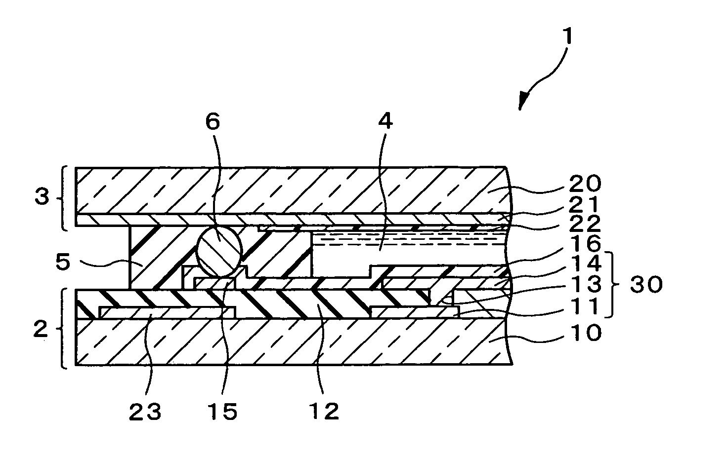
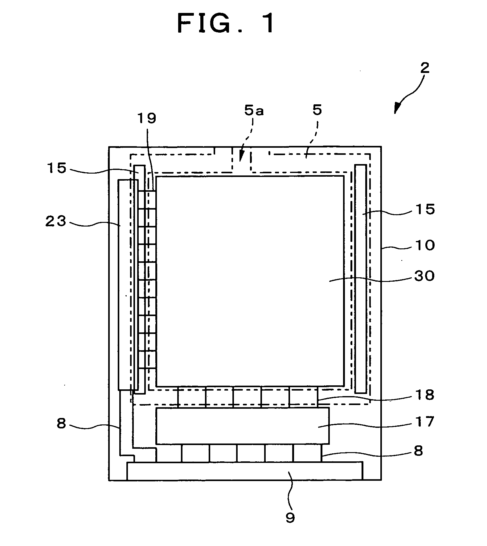
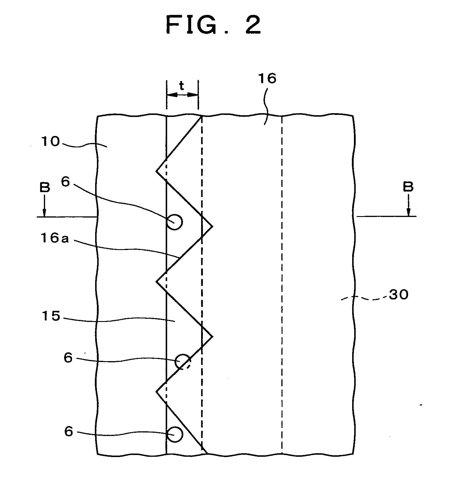
[0058] Liquid crystal display devices constituting embodiments of the present invention will be described in concrete terms below with reference to the attached figures. First, the liquid crystal display device of the present invention will be described. FIG. 1 is a plan view showing the TFT substrate of the liquid crystal display device of the present embodiment, and FIG. 2 is an enlarged view of the same. Furthermore, FIG. 3 is a sectional view showing the electrically conducting parts of the liquid crystal display device of the present embodiment, and corresponds to a sectional view along line B-B in FIG. 2. In order to facilitate viewing of the figures, the insulating layer is omitted from FIG. 1, and only the conductive particles 6, transparent electrode 10, transfer electrode 15, alignment film 16, and pixel array 30 are shown in FIG. 2. As is shown in FIGS. 1 through 3, the liquid crystal display device 1 of the present embodiment is constructed as follows. The TFT substrate ...

second embodiment

[0078] Next, a liquid crystal display device constituting the present invention will be described. FIG. 9 is an enlarged plan view showing the TFT substrate of the liquid crystal display device of the present embodiment. Furthermore, in FIG. 9, constituent elements that are the same as those of the TFT substrate 2 shown in FIG. 2 are labeled with the same reference numerals, and a detailed description of such constituent members is omitted. Furthermore, in FIG. 9, in order to facilitate viewing of the figure, only the conductive particles 6, transparent substrate 10, transfer electrode 55, alignment film 16, and pixel array 30 are shown. In the liquid crystal display device of the present embodiment, as is shown in FIG. 9, a plurality of transfer electrodes 55 are formed locally, and the alignment film 16 is formed so as to avoid the transfer electrodes 55. Specifically, the transfer electrodes 55 are formed in the area of the cut-out part 16a of the alignment film 16. In this liqui...


PUM


Abstract

A cut-out part is formed in the end part of the alignment film of a TFT substrate located on the side of a transfer electrode, and this cut-out part is positioned on the transfer electrode. Furthermore, a sealing member composed of a resin that includes conductive particles is formed on the peripheral edge parts of the alignment film. In this case, the system is devised so that the transfer electrode is covered by the sealing member. Furthermore, the TFT substrate and counter substrate are pasted together by the sealing member, and the transfer electrode of the TFT substrate and the counter electrode of the counter substrate are connected to each other. Subsequently, a liquid crystal layer is sealed between the TFT substrate and the counter substrate to produce a liquid crystal display device. As a result, a liquid crystal display device with a narrow frame and high display quality can be obtained.

Description

BACKGROUND OF THE INVENTION [0001] 1. Field of the Invention [0002] The present invention relates to a liquid crystal display device in which alignment films are formed on the surfaces of substrates, and a method for manufacturing the same, and more particularly relates to a liquid crystal display device in which thin film transistors are formed as switching elements, and a method for manufacturing the same. [0003] 2. Description of the Related Art [0004] In a general liquid crystal display device, a voltage is applied to a liquid crystal layer sealed between a pair of substrates disposed facing each other, and images are displayed by varying the transmissivity of the light passing through this liquid crystal layer so that the relative brightness is controlled. For example, in the case of a liquid crystal display device using an active matrix driving system, a TFT substrate on which TFTs (thin film transistors) are formed and a counter substrate on which a transparent electrode is f...

Claims


Application Information

Patent Timeline
IPC IPC(8): G02F1/1339
CPCG02F1/1339G02F1/1337
Inventor SHIGEMURA, KOJIHIROYA, TSUTOMU
Owner NEC LCD TECH CORP
Why Eureka
Try Eureka