Segmented waveguide structures

a waveguide and segmentation technology, applied in the field of waveguides, can solve the problems of difficult to establish an electrical contact with the waveguide without causing large optical loss in the optical mode, particularly troublesome problem, and substantial optical loss associated with that metal, so as to achieve high index contrast, reduce reflection, and reduce reflection

Inactive Publication Date: 2006-10-19
CALIFORNIA INST OF TECH
View PDF99 Cites 26 Cited by
  • Summary
  • Abstract
  • Description
  • Claims
  • Application Information

AI Technical Summary

Benefits of technology

[0010] Another embodiment of the invention comprises a high index contrast waveguide structure for propagating a wavelength, λ, comprising an elongate waveguide portion and a plurality of segments extending from the elongate waveguide portion. The plurality of segments have periodicity so as to produce coherent scattering and reduce reflection. The high index waveguide structure further comprises cladding disposed about the elongate waveguide portion. The elongate waveguide portion and the cladding have sufficiently high index contrast so as to support an optical mode having a full width half maximum intensity having a width of about twice the wavelength, λ, or less. In one embodiment, for example, the width of the full width

Problems solved by technology

One of the outstanding problems of this geometry, however, is the difficulty of establishing an electrical contact with the waveguide without causing large losses in the optical mode.
This problem is particularly troublesome when a DC or RF electrical field is to be appl

Method used


Image

  • Segmented waveguide structures
  • Segmented waveguide structures
  • Segmented waveguide structures

Examples


Embodiment Construction

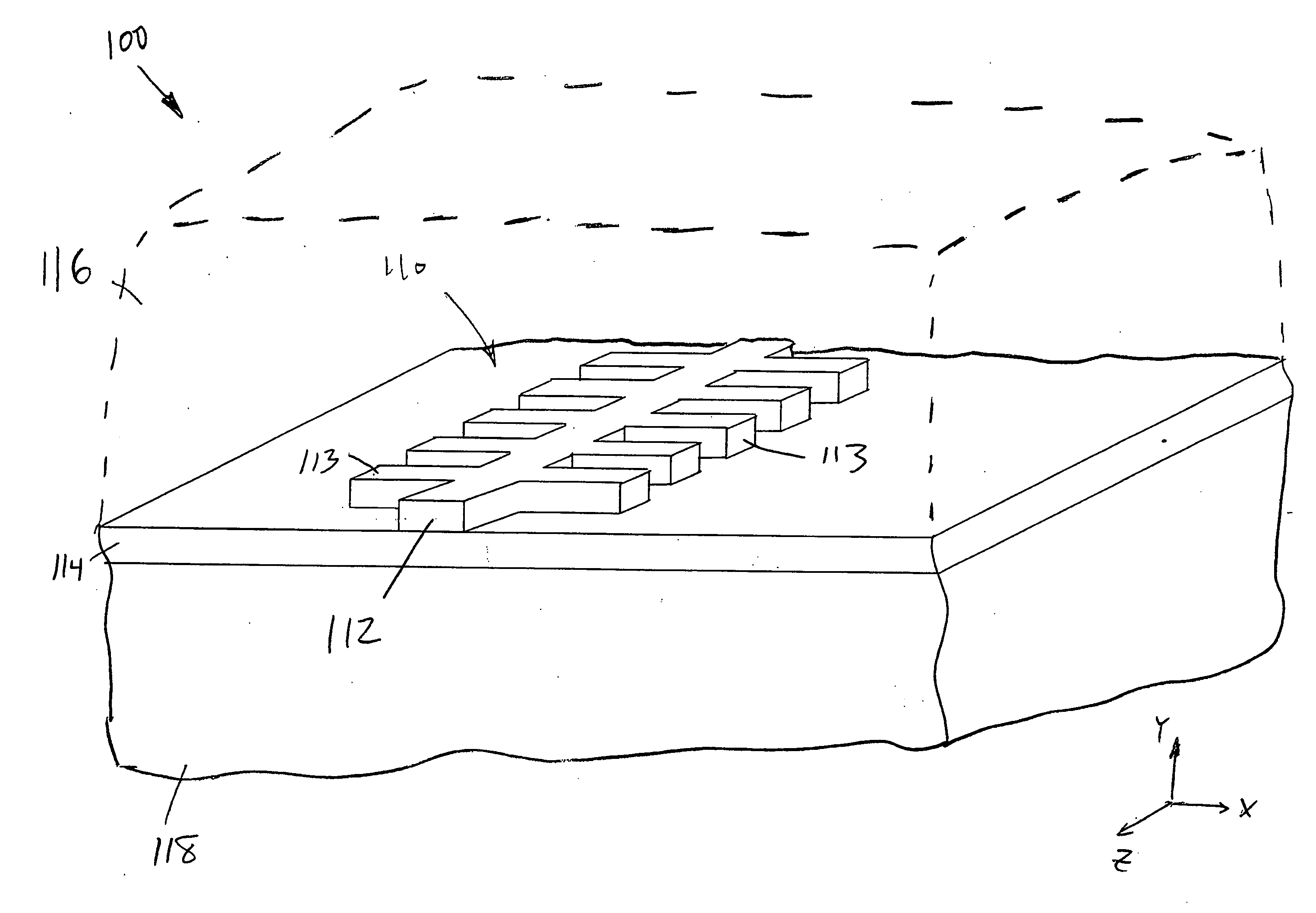
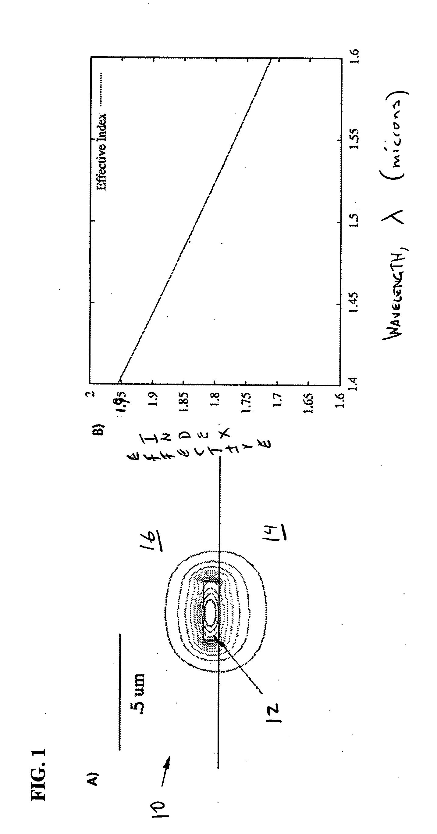
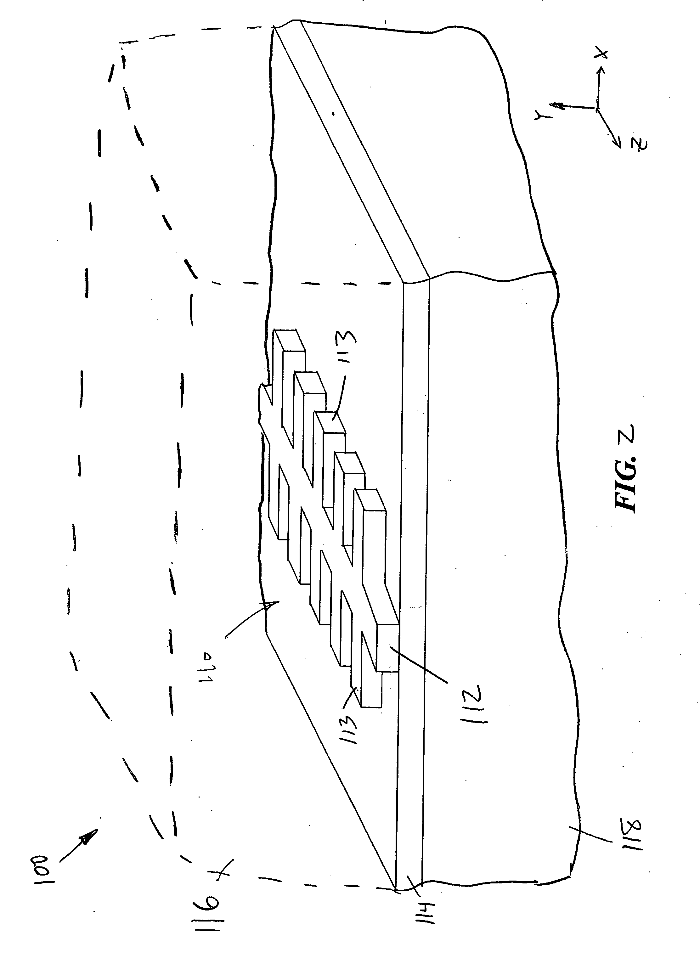
[0025] A high index contrast waveguide 10 having an SOI (Silicon-on-Insulator) geometry is shown in FIG. 1A. This waveguide 10 comprises a core region 12 comprising silicon disposed on a silicon dioxide layer 14. The silicon dioxide layer 14 is cladding for the core region 12. Additional cladding 16 is disposed about the core region 12. The silicon dioxide layer 14 may be disposed on a silicon handle (not shown) comprising, e.g., a 400 or 800 micron thick silicon substrate that provides mechanical support. The silicon in the core region 12 has an index of refraction of about 3.5. The silicon dioxide has an index of about 1.43. The additional cladding may comprise polymethylmethacrylate (PMMA), which has an index of refraction of about 1.43. Other materials may also be used to fabricate the waveguide 10.

[0026] The core region 12 as well as the cladding 14, 16 may comprises different materials. The core region may comprise III-V materials in some embodiments. Other materials may also...


PUM


Abstract

Various embodiment comprise silicon-on-insulator waveguide designs that simultaneously achieve both high optical confinement, low-loss, and provide for electrical connections. In certain embodiments, high index contrast waveguides comprise a central elongate waveguide portion and a segmented portion comprising a single thin layer of Silicon-On-Insulator that achieves both high optical confinement and minimal insertion loss. Other devices, such as chemical and biological sensors, and optical elements may also be fabricated.

Description

PRIORITY APPLICATION [0001] This application claims priority under 35 U.S.C. § 119(e) from U.S. Provisional Patent Application Ser. No. 60 / 577,905, entitled “Segmented Waveguides in Thin Silicon on Insulator” and filed Jun. 7, 2004 (Docket No. CIT-4131), which is hereby incorporated by reference herein in its entirety.STATEMENT REGARDING FEDERALLY SPONSORED R&D [0002] This invention was made with U.S. Government support under contract No. N00421-02-D-3223 awarded by the Naval Air Warfare Center Aircraft Division. The U.S. Government has a nonexclusive paid-up license in this invention.BACKGROUND [0003] 1. Field of the Invention [0004] The present invention is directed to waveguides, and more particularly, to waveguide structures incorporating a plurality of laterally extending segments. [0005] 2. Description of the Related Art [0006] Low loss single-mode waveguides in thin Silicon-On-Insulator (SOI) have been demonstrated. Such waveguides may comprise, for example, a patterned silic...

Claims


Application Information

Patent Timeline
IPC IPC(8): G02B6/10
CPCB82Y10/00B82Y20/00G01N21/66G01N21/774G01N2021/7776G02B6/124
Inventor HOCHBERG, MICHAELBAEHR-JONES, TOMWALKER, CHRISWITZENS, JEREMYGUNN, LAWRENCESCHERER, AXEL
Owner CALIFORNIA INST OF TECH
Why Eureka
Try Eureka