
Quality control system, quality control method, and method of lot-to-lot wafer processing

Inactive Publication Date: 2006-10-19
KK TOSHIBA
View PDF8 Cites 23 Cited by
  • Summary
  • Abstract
  • Description
  • Claims
  • Application Information

AI Technical Summary

Benefits of technology

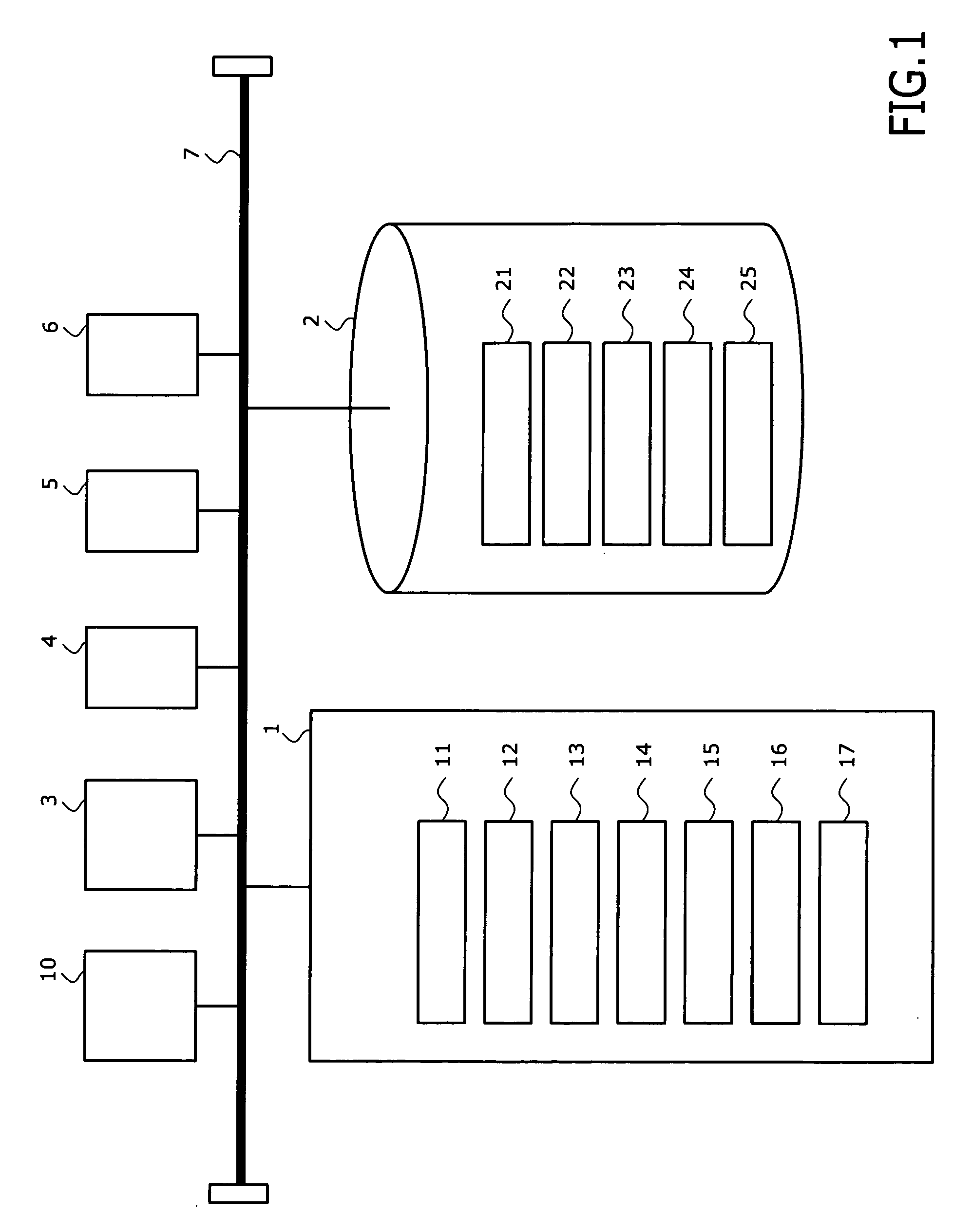
[0008] According to an aspect of the invention, there is provided a quality control system comprising: a quality control value storage unit configured to store quality control actual measurements of past lots; a data acquisition device configured to acquire device internal information of a processing device that processes an intended lot; a device internal information storage unit configured to store the device internal information; a recipe storage unit configured to store a plurality of recipes, each recipe having a mutually different distribution of sampling density within a wafer; a quality control value prediction unit configured to read the device internal information from the device internal information storage unit, reading the quality control actual measurements of past lots from the quality control value storage unit, and predicting a quality control prediction value of the intended lot using the device internal information and the quality control actual measurements; a wafer determination unit configured to determine a sample wafer to be measured from among a plurality of wafers constituting the intended lot using the quality control prediction value; a recipe selection unit configured to read the plurality of recipes from the recipe storage unit and selecting an application recipe to be applied to the sample wafer from among the plurality of recipes using the quality control prediction value; and a measurement device configured to use the application recipe to make a quality control measurement on the sample wafer and storing a measurement result in the quality control value storage unit.
[0009] According to other aspect of the invention, there is provided a quality control method comprising: acquiring device internal information of a processing device that processes an intend

Problems solved by technology

This causes within-lot variation due to the parameter fluctuation of the semiconductor manufacturing devices before and after seasoning.
Thus, defective lots may be missed.

Method used


Image

  • Quality control system, quality control method, and method of lot-to-lot wafer processing
  • Quality control system, quality control method, and method of lot-to-lot wafer processing
  • Quality control system, quality control method, and method of lot-to-lot wafer processing

Examples


first embodiment

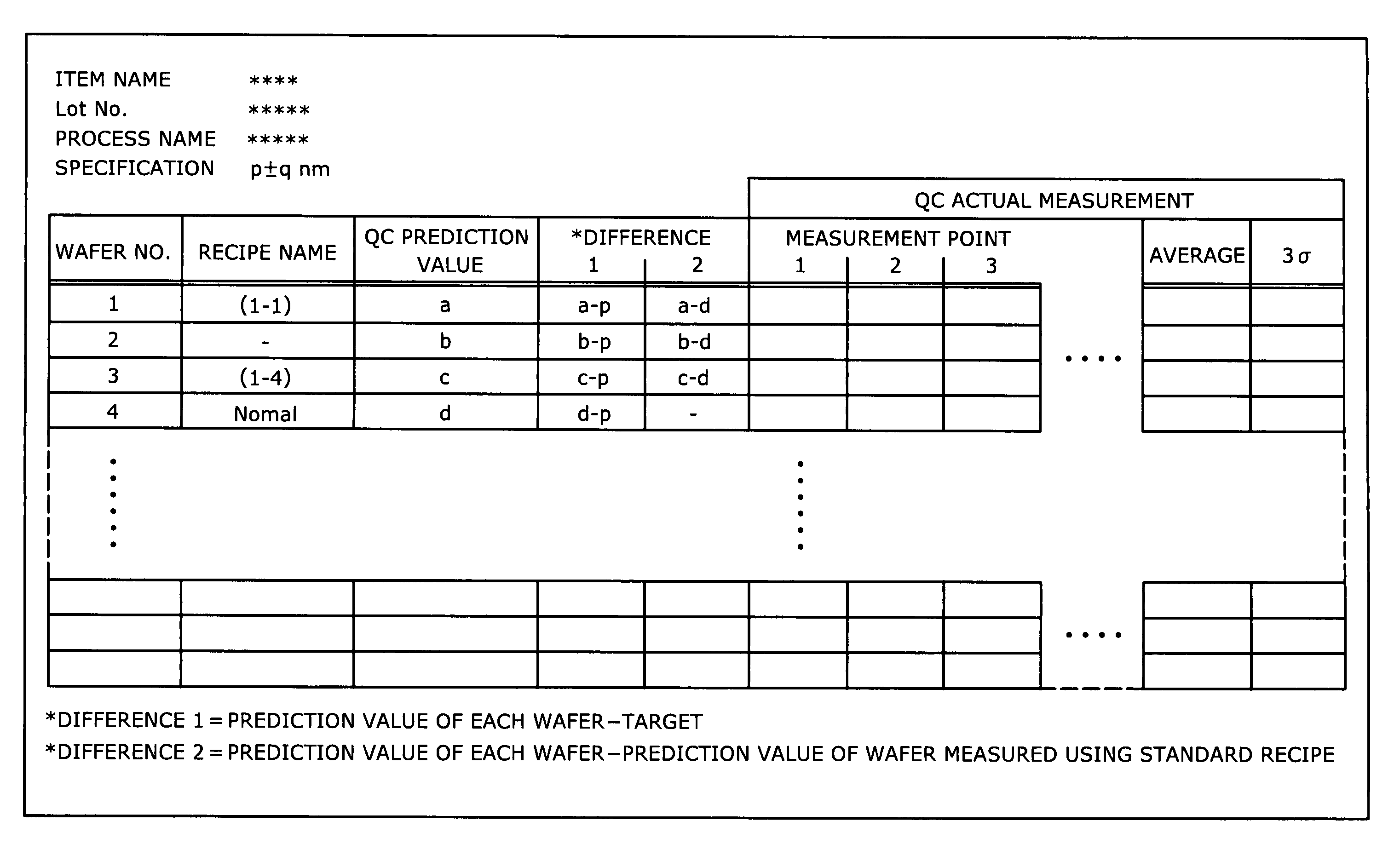
[0035] As shown in FIG. 1, the quality control system in accordance with the first embodiment of the invention comprises a QC value storage unit 22 that stores QC actual measurements of past lots, a data acquisition device 3 that acquires in real time the device internal information of a processing device 10 processing an intended lot, a device internal information storage unit 21 that stores the device internal information, a recipe storage unit 24 that stores a plurality of recipes classified by the distribution of sampling density within a wafer, a QC value prediction unit 11 that reads the device internal information and the QC actual measurements of past lots from the device internal information storage unit 21 and the QC value storage unit 22, respectively, and predicts a QC prediction value of the intended lot using the device internal information and the QC actual measurements, a wafer determination unit 12 that determines a sample wafer to be measured from among a plurality...

second embodiment

[0076] As shown in FIG. 29, the quality control system in accordance with the second embodiment of the invention is different from the quality control system shown in FIG. 1 in that the data storage device 2a further comprises a non-defectives data storage unit 26 and defectives data storage unit 27, and that the CPU la further comprises a control width determination unit 18.

[0077] The control width determination unit 18 determines a “control width” used in FDC and statistical process control (SPC). In “FDC”, as in the FDC unit 17, the processing device 10 is continuously monitored while it processes wafers as part of the process of manufacturing semiconductor devices. Before any deviation of processing conditions in the processing device 10 adversely affects the product yield, the processing device 10 can be shut down to reduce risk on the wafers. In “SPC”, an enormous amount of data collected at various checkpoints in the manufacturing process is used for statistical processing t...


PUM


Abstract

A quality control system has: a QC value storage unit that stores QC actual measurements of past lots, a data acquisition device that acquires the device internal information of a processing device processing an intended lot, a device internal information storage unit that stores the device internal information, a recipe storage unit that stores a plurality of recipes classified by the distribution of sampling density within a wafer, a QC value prediction unit that predicts a QC prediction value of the intended lot using the device internal information and the QC actual measurements, a wafer determination unit that determines a sample wafer to be measured from among a plurality of wafers constituting the intended lot using the QC prediction value, a recipe selection unit that selects an application recipe to be applied to the sample wafer from among the plurality of recipes using the QC prediction value, and a measurement device that makes a QC measurement on the sample wafer using the application recipe and stores the measurement result in the QC value storage unit.

Description

CROSS-REFERENCE TO RELATED APPLICATIONS [0001] This application is based upon and claims the benefit of priority from the prior Japanese Patent Application No. 2005-109209, filed on Apr. 5, 2005; the entire contents of which are incorporated herein by reference. BACKGROUND OF THE INVENTION [0002] 1. Field of the Invention [0003] This invention relates to a quality control system, a quality control method, and a method of lot-to-lot wafer processing, and more particularly to a quality control system, a quality control method, and a method of lot-to-lot wafer processing being applied to the technology of manufacturing semiconductor devices for providing lot quality control. [0004] 2. Background Art [0005] Semiconductor devices are manufactured by numerous semiconductor manufacturing devices in a long, complicated series of numerous steps including lithography, etching, heat treatment (oxidation, annealing, and diffusion), ion implantation, thin film formation (CVD (Chemical Vapor Depo...

Claims


Application Information

Patent Timeline
IPC IPC(8): G06F19/00G01M99/00G05B19/418H01L21/02
CPCG05B19/41875G05B2219/32097H01L21/67253G05B2219/45031G05B2219/32194Y02P90/02
Inventor OGAWA, AKIRAUSHIKU, YUKIHIROINO, TOMOMI
Owner KK TOSHIBA
Learn More