Multi-bit non-volatile memory device having a dual-gate and method of manufacturing the same, and method of multi-bit cell operation

a non-volatile memory, multi-gate technology, applied in the direction of semiconductor devices, electrical devices, nanotechnology, etc., can solve the problems of short channel effect, shrinkage of device size, increased leakage current,

Active Publication Date: 2006-10-26
KOREA ADVANCED INST OF SCI & TECH
View PDF3 Cites 142 Cited by
  • Summary
  • Abstract
  • Description
  • Claims
  • Application Information

AI Technical Summary

Benefits of technology

[0019] The method may further comprise the step of depositing a screen oxide layer on the dual gate, injecting ion and then removing the screen

Problems solved by technology

However, in the case where a device structure of an existing 2 dimensional channel is employed, a short channel effect, such as an increase in the leakage current, is generated when the device si

Method used


Image

  • Multi-bit non-volatile memory device having a dual-gate and method of manufacturing the same, and method of multi-bit cell operation
  • Multi-bit non-volatile memory device having a dual-gate and method of manufacturing the same, and method of multi-bit cell operation
  • Multi-bit non-volatile memory device having a dual-gate and method of manufacturing the same, and method of multi-bit cell operation

Examples


Embodiment Construction

[0052] In the following detailed description, only certain exemplary embodiments of the present invention have been shown and described simply by way of illustration. As those skilled in the art will realize, the described embodiment may be modified in various different ways, all without departing from the spirit or scope of the present invention. Accordingly, the drawings and description are to be regarded as illustrative in nature and not restrictive. Like reference numerals designate like elements throughout.

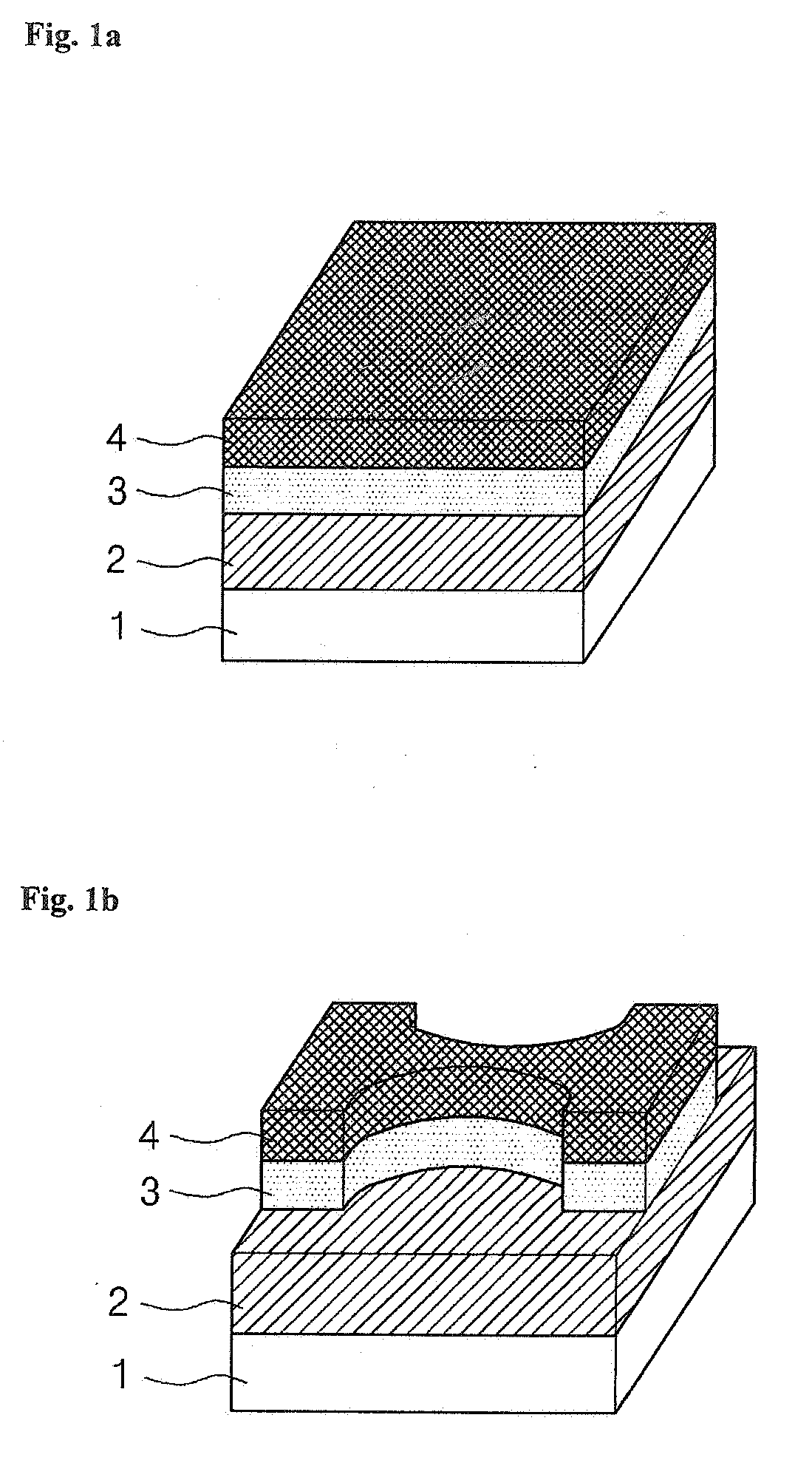
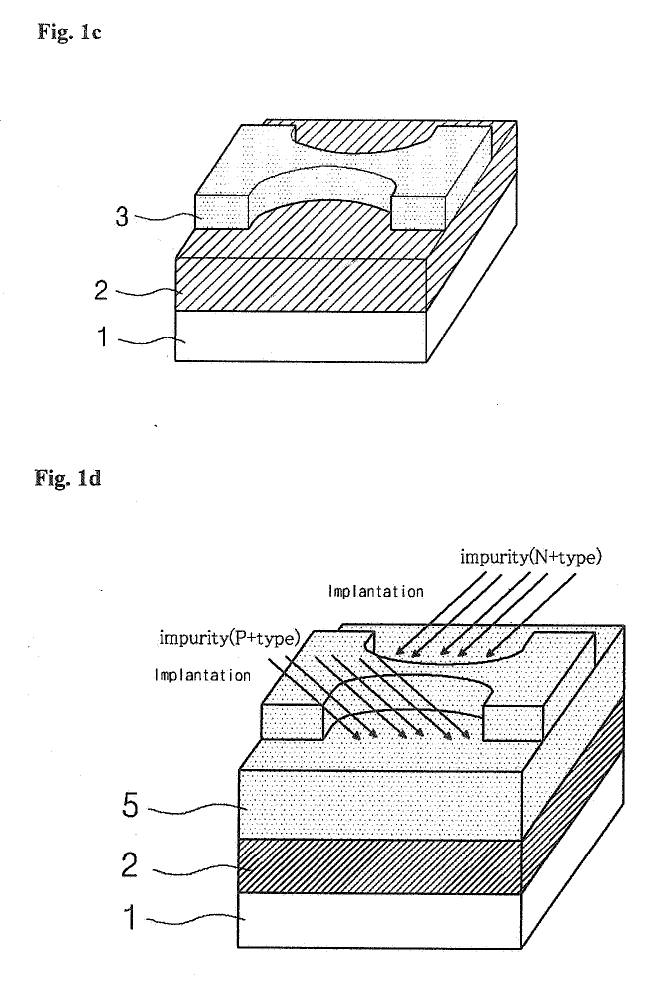
[0053]FIGS. 1a to 1g are perspective views sequentially illustrating a method of manufacturing a multi-bit non-volatile memory device having a dual gate structure according to an embodiment of the present invention.

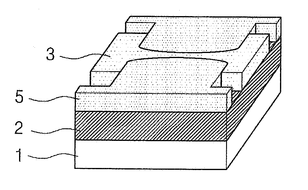
[0054] Referring to FIG. 1a, to fabricate the multi-bit non-volatile memory device having the dual gate structure, a silicon substrate 1, a lower insulating film 2, silicon 3 and a hard mask 4 are sequentially laminated. The hard mask 4 may be formed using a mate...


PUM


Abstract

The present invention relates to a multi-bit non-volatile memory device having a dual gate employing local charge trap and method of manufacturing the same, and an operating method for a multi-bit cell operation.

Description

[0001] This Nonprovisional application claims priority under 35 U.S.C. §119(a) on Patent Application No. 10-2005-0033697 filed in Korea on Apr. 22, 2005, the entire contents of which are hereby incorporated by reference. BACKGROUND [0002] 1. Field of the Invention [0003] The present invention relates to non-volatile memory devices and method of manufacturing the same. More particularly, the present invention relates to a multi-bit non-volatile memory device having a dual gate structure, and method of manufacturing the same, and an operating method for a multi-bit cell operation. [0004] 2. Discussion of Related Art [0005] A flash memory, i.e., a non-volatile memory device in which data can be electrically programmed / erased / read can be higher integrated and have a superior data integrity. Therefore, the flash memory can be used as an auxiliary memory of a system and can also be applied to DRAM interface. [0006] The flash memory has been designed toward a direction in which the level o...

Claims


Application Information

Patent Timeline
IPC IPC(8): H01L29/788H01L21/336
CPCH01L29/4232H01L29/7923H01L29/785H01L29/66795B82Y10/00
Inventor CHOI, YANG-KYULEE, HYUNJIN
Owner KOREA ADVANCED INST OF SCI & TECH
Why Eureka
Try Eureka