
Logic device with low EMI

Active Publication Date: 2006-11-02
XIAMEN XM PLUS TECH LTD
View PDF3 Cites 2 Cited by
  • Summary
  • Abstract
  • Description
  • Claims
  • Application Information

AI Technical Summary

Benefits of technology

[0008] In accordance with one aspect of the present invention, there is provided a logic device with low electromagnetic interference (EMI). The logic device includes a digital logic gate and a current-limited circuit. The digital logic gate provides a corresponding digital logic function. The current-limited circuit is connected to the digital logic gate in order to provide a fixed current to the digital logic gate to thus reduce a transient current of the digital logic gate. Accordingly, an electromagnetic interface (EMI) caused by switching of the digital logic gate is reduced.
[0009] In accordance with another aspect of the present invention, there is provided a logic device with low electromagnetic interference (EMI). The logic device includes a current mirror circuit, a digital logic gate, a voltage-limited circuit and a current-limited circuit. The current mirror circuit is connected to a high potential and provides a fixed current through a node A. The digital logic gate provides a corresponding digital logic function. The voltage-limited circuit is connected to the current mirror circuit and the digital logic gate through the node A, and limits the voltage of node A to a fixed voltage in order to provide the fixed voltage to the digital logic gate to thereby reduce an output voltage swing of the digital logic gate. The current-limited circuit is connected to the current mirror circuit and the digital logic gate via the node A in order to provide a fixed current to the digital logic gate to thus reduce a transient current of the digital logic gate. Accordingly, an electromagnetic interface (EMI) caused by switching of the digital logic gate is reduced with the reduced output voltage swing and transient current.

Problems solved by technology

Due to increasingly powerful functions of current electronic products, the associated circuitry is becoming more and more complicated.
Therefore, the EMI causes an essential problem in the design of electronic products.
However, such a long channel of transistor technology increases the cost due to the increased area required for the logic gate, which is caused by the increased channel length.
In addition, when the process is changed, re-adjusting the channel length of a transistor is required, so as to increase the processing complexity.

Method used


Image

  • Logic device with low EMI
  • Logic device with low EMI
  • Logic device with low EMI

Examples


Embodiment Construction

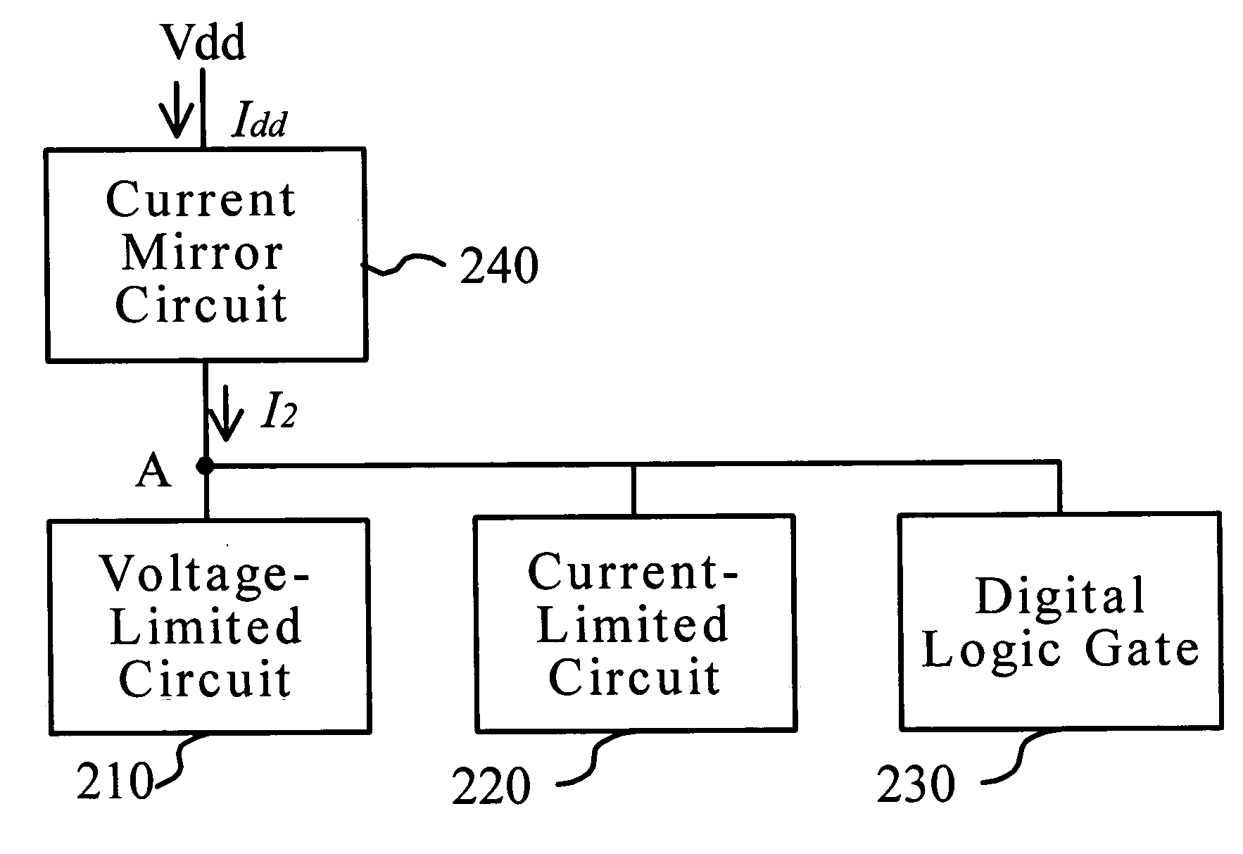
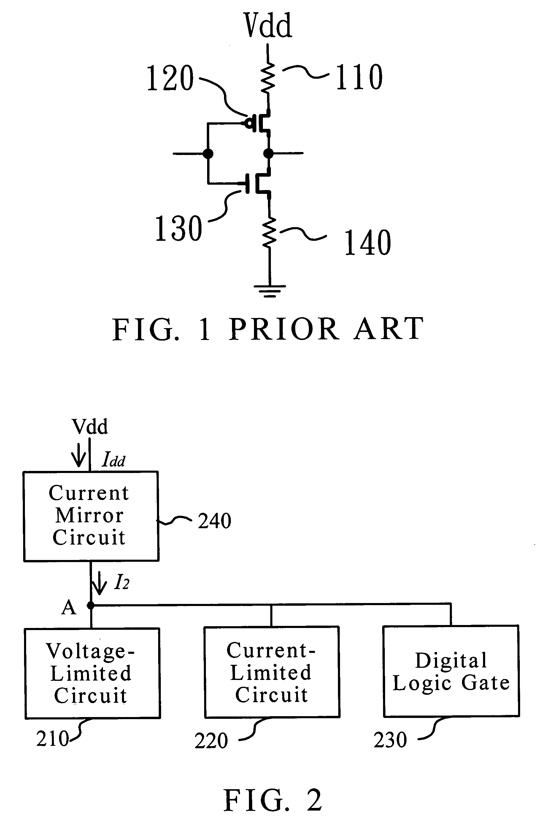
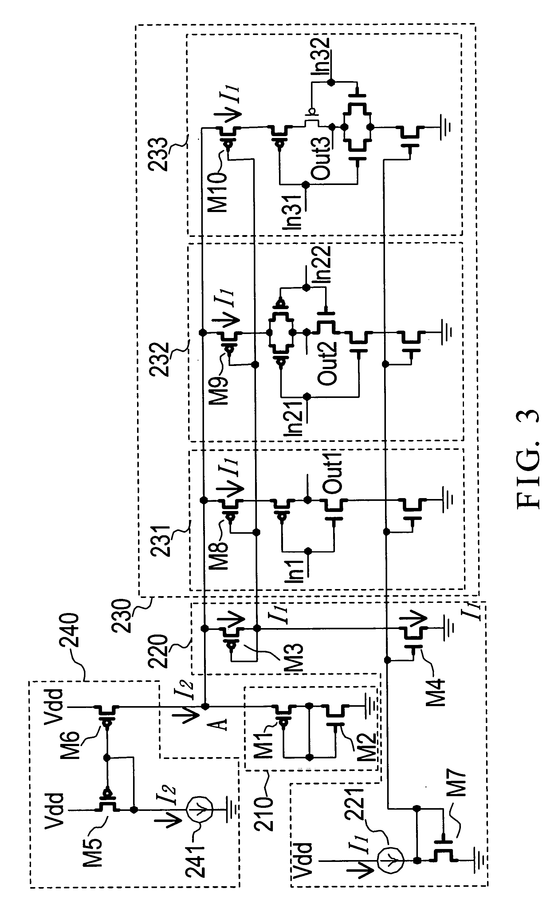
[0019]FIG. 2 is a block diagram of a logic device with low EMI in accordance with the invention. As shown in FIG. 2, the logic device includes a current mirror circuit 240, a digital logic gate 230, a voltage-limited circuit 210 and a current-limited circuit 220. The current mirror circuit 240 is connected to a high potential Vdd. Thus, an input current Idd is inputted to the current mirror circuit 240, and a fixed current I2 is output to a node A by the current mirror circuit 240.

[0020] The digital logic gate 230 provides a corresponding digital logic function. The digital logic gate 230 can be a NOT gate 231, a NAND gate 232, a NOR gate 233, or a combination cited above.

[0021] The voltage-limited circuit 210 is connected to the current mirror circuit 240 and the digital logic gate 230 through the node A in order to provide a fixed voltage to the digital logic gate 230 to thus reduce an output voltage swing of the digital logic gate 230. Accordingly, an electromagnetic interferen...


PUM


Abstract

A logic device with low electromagnetic interference. The logic device includes a digital logic gate, a voltage-limited circuit and a current-limited circuit. The digital logic gate provides a corresponding digital logic function. The voltage-limited circuit is connected to the digital logic gate in order to provide a fixed voltage to the digital logic gate to thus reduce an output voltage swing of the digital logic gate. The current-limited circuit is connected to the digital logic gate in order to provide a fixed current to the digital logic gate to thus reduce a transient current of the digital logic gate. Accordingly, an electromagnetic interface (EMI) caused by switching of the digital logic gate is reduced with the reduced output voltage swing and transient current.

Description

BACKGROUND OF THE INVENTION [0001] 1. Field of the Invention [0002] The invention relates to a digital logic gate and, more particularly, to a logic device with low electromagnetic interference (EMI). [0003] 2. Description of Related Art [0004] Due to increasingly powerful functions of current electronic products, the associated circuitry is becoming more and more complicated. For a good electronic product, in addition to the inherent functions, an electromagnetic interference (EMI) has a key impact on the product quality and technical capability indication. Therefore, the EMI causes an essential problem in the design of electronic products. A circuit designer uses an advanced CAD tool to widen the capability of work in the design of electronic circuits, but to give the little help with the EMI problem. [0005] A typical technology uses long channel of PMOS or NMOS transistors to reduce the transient current in a logic gate to thus reduce the EMI problem in the logic gate. However, s...

Claims


Application Information

Patent Timeline
IPC IPC(8): H03K19/003
CPCH03K19/00361
Inventor WANG, YAO-CHICHANG, YING-TANGPAN, CHING-WENYU, CHIN-PIN
Owner XIAMEN XM PLUS TECH LTD
Learn More