Organic electroluminescent display

a technology of organic electroluminescent display and organic electroluminescent display, which is applied in the direction of electric variable regulation, process and machine control, instruments, etc., can solve the problems of non-uniform brightness of active matrix organic electroluminescent display, inability to check for progressive defects in organic electroluminescent display

Active Publication Date: 2006-11-02
SAMSUNG DISPLAY CO LTD
View PDF4 Cites 80 Cited by
  • Summary
  • Abstract
  • Description
  • Claims
  • Application Information

AI Technical Summary

Problems solved by technology

However, the active matrix organic electroluminescent display has non-uniform brightness.
Thus, the pixels display different brightness with regard to the same data signal, thereby allowing the whole image display region to have non-uniform brightness.
However, this method cannot check for progressive defects in the organic electroluminescent display, and must drive a plurality of transistors corresponding to the pixels.

Method used


Image

  • Organic electroluminescent display
  • Organic electroluminescent display
  • Organic electroluminescent display

Examples


first embodiment

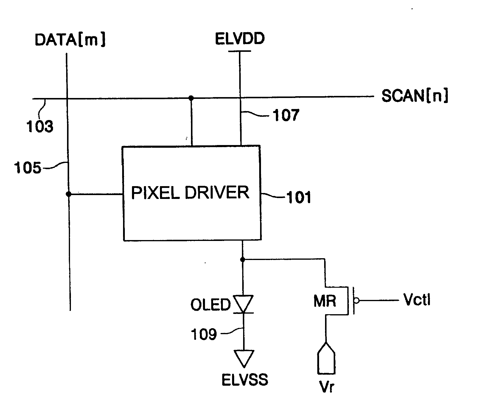
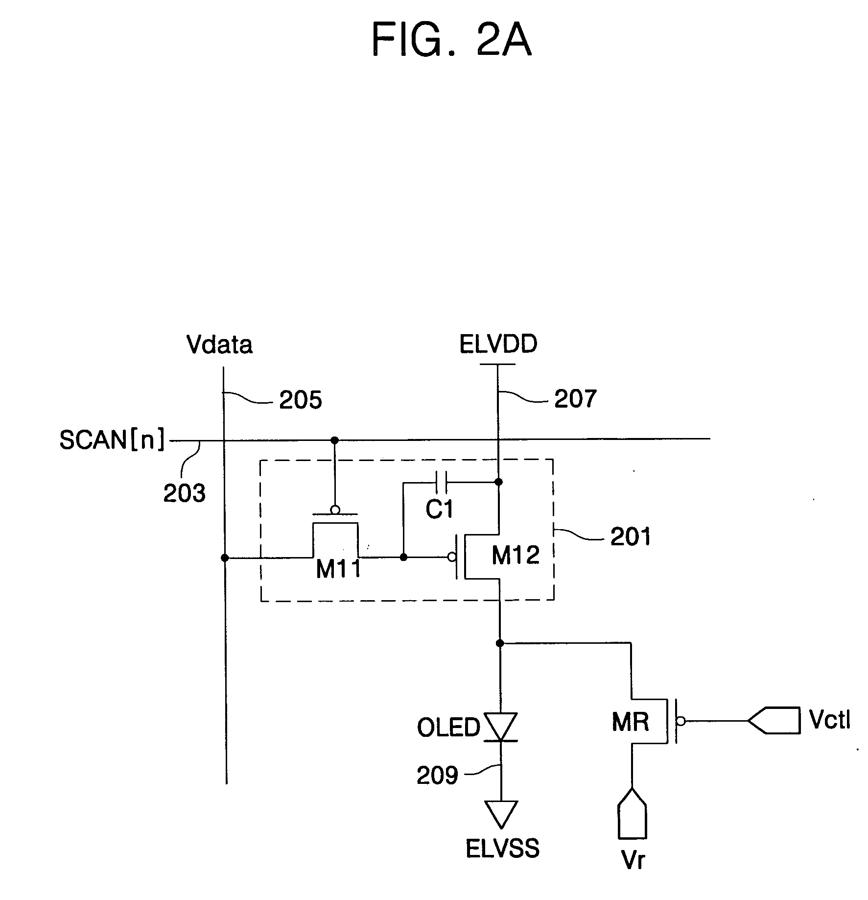
[0032]FIG. 1 is a block diagram of an organic electroluminescent display according to the present invention.

[0033] Referring to FIG. 1, the organic electroluminescent display according to the first embodiment of the present invention includes a pixel driving part 101, an OLED, and a reverse bias transistor MR.

[0034] The pixel driving part 101 includes a plurality of transistors and a capacitor. Furthermore, the pixel driving part 101 is formed in a region where a scan line 103 intersects a data line 105. When a scan signal SCAN[n] is supplied from the scan line 103, the pixel driving part 101 is selected and a data signal DATA[m] is supplied to the selected pixel driving part 101. The data signal DATA[m] is supplied to the pixel driving part 101 through the data line 105. The data signal DATA[m] supplied to the pixel driving part 101 is stored as a voltage in the capacitor provided in the pixel driving part 101. Alternatively, the data signal DATA[m] can be supplied as a current to...

second embodiment

[0061]FIG. 3 is a block diagram of an organic electroluminescent display according to the present invention.

[0062] Referring to FIG. 3, the organic electroluminescent display according to the second embodiment of the present invention includes a pixel driving part 301, an OLED, and a reverse bias transistor MR.

[0063] The pixel driving part 301 includes a plurality of transistors and a capacitor. Furthermore, the pixel driving part 301 is formed in a region where a scan line 303 intersects a data line 305. When a scan signal SCAN[n] is supplied from the scan line 303, the pixel driving part 301 is selected and a data signal DATA[m] is supplied to the selected pixel driving part 301. The data signal DATA[m] is supplied to the pixel driving part 301 through the data line 305. The data signal DATA[m] supplied to the pixel driving part 301 is stored as a voltage in the capacitor provided in the pixel driving part 301. Alternatively, the data signal DATA[m] can be supplied as a current t...

third embodiment

[0080]FIG. 5 is a block diagram of an organic electroluminescent display according to the present invention.

[0081] Referring to FIG. 5, the organic electroluminescent display according to the third embodiment of the present invention includes a pixel driving part 501, an OLED, a first reverse bias transistor MR1, and a second reverse bias transistor MR2.

[0082] The pixel driving part 501 is selected by a scan signal SCAN[n] supplied through a scan line 503, and receives a data signal DATA[m] through a data line 505. The data signal DATA[m] is either a data voltage or a data current. Furthermore, the pixel driving part 501 is connected to a first power line 507 and supplies a positive source voltage ELVDD from the first power line 507 to the OLED, thereby making the OLED emit light.

[0083] The OLED is connected between the pixel driving part 501 and a second power line 509. That is, the OLED has an anode connected to the pixel driving part 501, and a cathode electrode connected to th...


PUM


Abstract

An organic electroluminescent display supplies a reverse bias voltage to an Organic Light-Emitting Diode (OLED) for emitting light. The organic electroluminescent display additionally includes a reverse bias transistor to supply the reverse bias voltage. The reverse bias transistor is connected between an anode of the OLED and a reverse bias power supply, between the anode of the OLED and a first power line supplying a positive source voltage, or between the anode of the OLED and a data line. Furthermore, the reverse bias transistor can be connected between an initialization line and the anode of the OLED. The reverse bias voltage is supplied to the OLED before displaying an image or within a non-display period of a vertical synchronous signal, thereby enabling detection of whether or not the OLED has a defect.

Description

CLAIM OF PRIORITY [0001] This application makes reference to, incorporates the same herein, and claims all benefits accruing under 35 U.S.C. §119 from an application for ORGANIC ELECTROLUMINESCENT DISPLAY earlier filed in the Korean Intellectual Property Office on Apr. 29, 2005 and there duly assigned Serial No. 10-2005-0036394. BACKGROUND OF THE INVENTION [0002] 1. Field of the Invention [0003] The present invention relates to an organic electroluminescent display, and more particularly, to an organic electroluminescent display with a pixel circuit for supplying a reverse bias voltage to an Organic Light-Emitting Diode (OLED) provided in a pixel. [0004] 2. Description of the Related Art [0005] An organic electroluminescent display displays an image by supplying a data signal to a self-emissive OLED, and is classified as either a passive matrix or an active matrix organic electroluminescent display according to a driving method. [0006] In a passive matrix organic electroluminescent ...

Claims


Application Information

Patent Timeline
Patent Type & Authority Applications(United States)
IPC IPC(8): G09G3/30H05B44/00
CPCG09G3/006G09G3/3233G09G3/325G09G3/3283G09G2310/0256G09G2300/0814G09G2300/0819G09G2300/0861G09G2330/02G09G3/3291G09G3/3241E03B11/02B65D90/041
Inventor KOMIYA, NAOAKI
Owner SAMSUNG DISPLAY CO LTD
Why Eureka
Try Eureka