Load lock apparatus, load lock section, substrate processing system and substrate processing method

a technology of loading apparatus and load lock section, which is applied in the direction of electrical apparatus, conveyor parts, thin material processing, etc., can solve the problems of substrate warpage, difficult to efficiently heat or cool the substrate, and substrate breakage, so as to reduce the temperature difference, prevent the substrate from deformation, and reduce the effect of substrate deformation

Inactive Publication Date: 2006-11-02
TOKYO ELECTRON LTD
View PDF12 Cites 156 Cited by
  • Summary
  • Abstract
  • Description
  • Claims
  • Application Information

AI Technical Summary

Benefits of technology

[0011] Another load lock apparatus of the present invention is a load lock apparatus including a carry-out port provided on a side of a carry-in/out section for carrying in/out a substrate, a carry-in port provided on a side of a processing section for processing the substrate, and supporting members for supporting the substrate, the apparatus including: a first cooling plate and a second cooling plate each for cooling the substrate supported on the supporting member

Problems solved by technology

However, it is difficult to efficiently heat or cool the substrate in the load lock section of the conventional processing system, and therefore it has been desired to efficiently heat or cool the substrate.
Further, the substrate has sometimes warped due to the

Method used


Image

  • Load lock apparatus, load lock section, substrate processing system and substrate processing method
  • Load lock apparatus, load lock section, substrate processing system and substrate processing method
  • Load lock apparatus, load lock section, substrate processing system and substrate processing method

Examples


Embodiment Construction

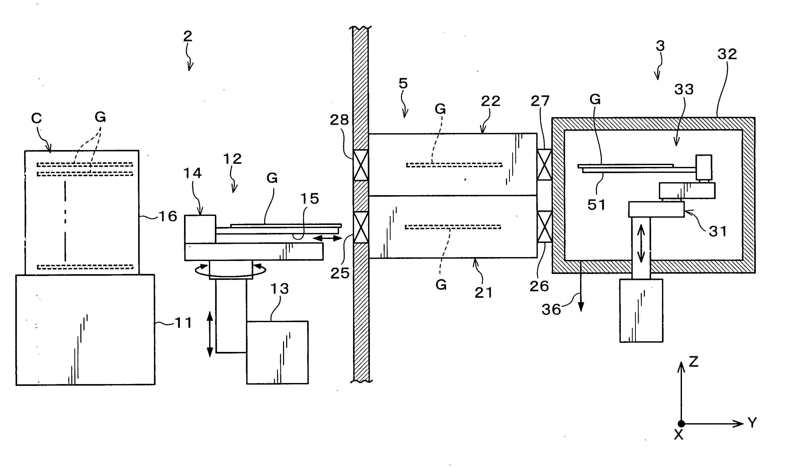
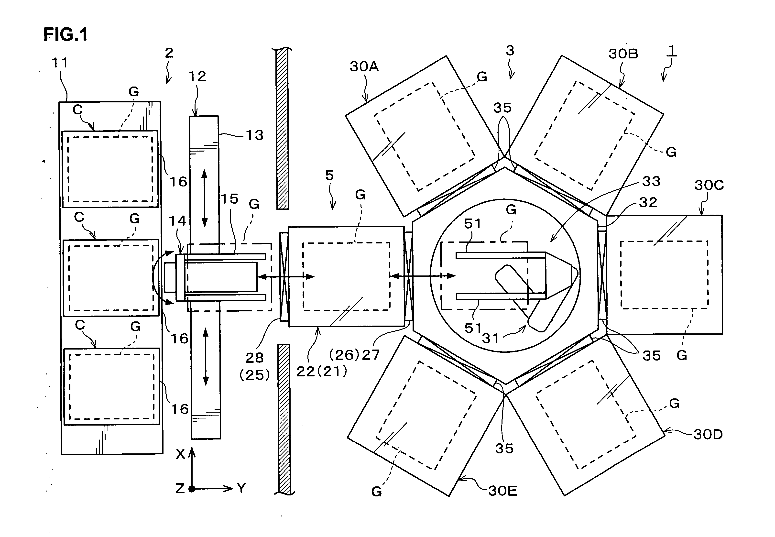
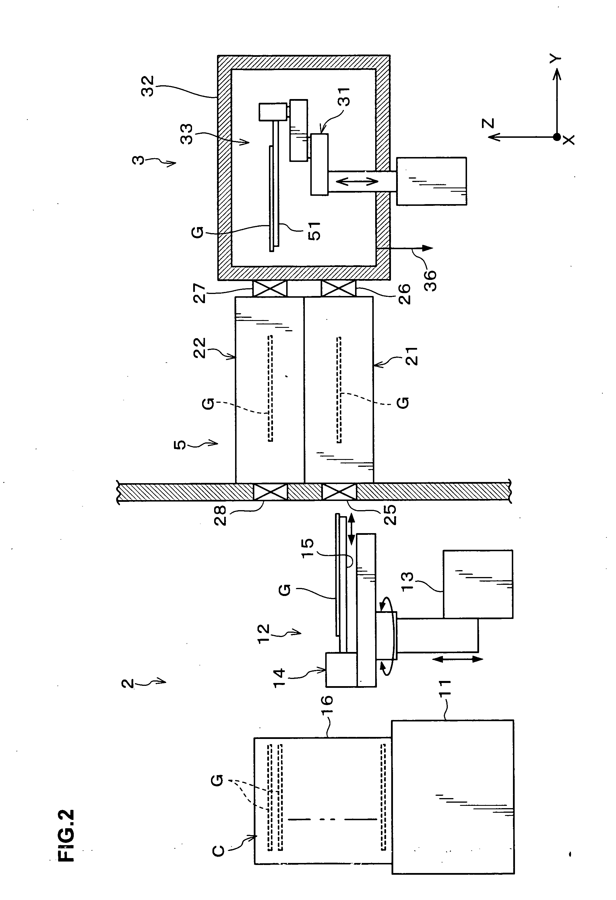
[0025] Hereinafter, a preferred embodiment of the present invention will be described based on a processing system which embodies processes of forming a thin film by plasma CVD (Chemical Vapor Deposition) processing for a glass substrate G for LCD (Liquid Crystal Display) as an example of a substrate. FIG. 1 is a plan view showing a schematic configuration of a processing system 1 according to the embodiment of the present invention. The processing system 1 shown in FIG. 1 is a so-called multi-chamber type processing system which includes a carry-in / out section 2 for carrying in / out the substrate G to / from the outside of the processing system 1; a processing section 3 for performing CVD processing for the substrate G; and a load lock section 5 arranged between the carry-in / out section 2 and the processing section 3.

[0026] In the carry-in / out section 2, a mounting table 11 on which cassettes C housing a plurality of substrates G are mounted and a first carrier unit 12 for carrying t...


PUM


Abstract

A substrate processing system including a processing section for processing a substrate; a carry-in/out section for carrying in/out the substrate; and a load lock section provided between the processing section and the carry-in/out section, is characterized in that the load lock section includes a first load lock apparatus including a carry-in port provided on a side of the carry-in/out section for carrying in/out the substrate, a carry-out port provided on a side of the processing section for processing the substrate, and supporting members for supporting the substrate; and a second load lock apparatus including a carry-out port provided on the carry-in/out section side, a carry-in port provided on the processing section side, and supporting members for supporting the substrate, that the second load lock apparatus includes a first cooling plate and a second cooling plate each for cooling the substrate supported on the supporting members, and that one of the first cooling plate and the second cooling plate is located on a front surface side of the substrate and another is located on a rear surface side of the substrate.

Description

BACKGROUND OF THE INVENTION [0001] 1. Field of the Invention [0002] The present invention relates to a substrate processing system for processing an LCD substrate or the like, and to a load lock section and a load lock apparatus each for carrying in / out the substrate to a substrate processing section, and further to a substrate processing method. [0003] 2. Description of the Related Art [0004] In a manufacturing process of, for example, an LCD substrate or the like, a so-called multi-chamber type processing system is used which includes a plurality of substrate processing apparatuses for performing predetermined processing for the substrate in a reduced-pressure atmosphere, such as etching, ashing, and so on (see Japanese Translated National Publication of Patent Application No. 2004-523880). Such a processing system includes a carrier room including a substrate carrier unit for carrying the substrate and a processing section having a plurality of substrate processing apparatuses pr...

Claims


Application Information

Patent Timeline
IPC IPC(8): H01L21/677
CPCH01L21/67201H01L21/67098H01L21/67742H01L21/68707Y10S414/139
Inventor IWABUCHI, KATSUHIKO
Owner TOKYO ELECTRON LTD
Why Eureka
Try Eureka