Transfer substrate, method for fabricating display device, and display device

a technology of transfer substrate and display device, which is applied in the direction of thermal imaging, natural mineral layered products, nuclear engineering, etc., can solve the problems of high cost, high cost, and inability to employ the method described above, and achieve high accuracy

Inactive Publication Date: 2006-11-02
JOLED INC
View PDF0 Cites 66 Cited by
  • Summary
  • Abstract
  • Description
  • Claims
  • Application Information

AI Technical Summary

Benefits of technology

[0022] In a display device fabricated using the transfer substrate or the fabrication method described above, it is

Problems solved by technology

However, in the method in which heat is directly applied to the transfer layer through the member having high thermal conductivity, the amount of thermal energy required is very large, and damage to the organic layer to be transferred is very h

Method used


Image

  • Transfer substrate, method for fabricating display device, and display device
  • Transfer substrate, method for fabricating display device, and display device
  • Transfer substrate, method for fabricating display device, and display device

Examples


Embodiment Construction

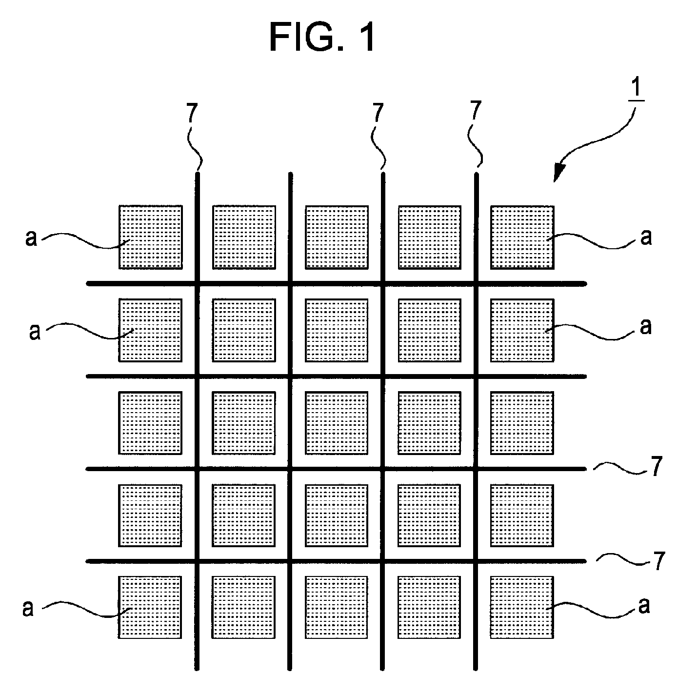
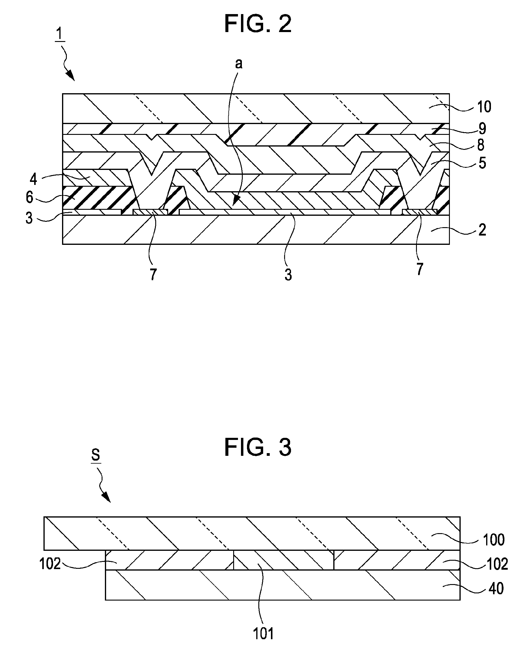
[0030] Embodiments of the present invention will be described below with reference to the drawings. FIG. 1 is a schematic view of a display device according to an embodiment of the present invention. An organic EL element 1 is provided correspondingly to each pixel a. As shown in FIG. 2 which is a schematic cross-sectional view, the organic EL element 1 includes a lower electrode 3, a functional layer 4, and an upper common electrode 5 provided in that order on a substrate 2. Furthermore, a protective film 8 is provided over the upper common electrode 5, and a glass substrate 10 is attached thereto through an UV curable resin 9.

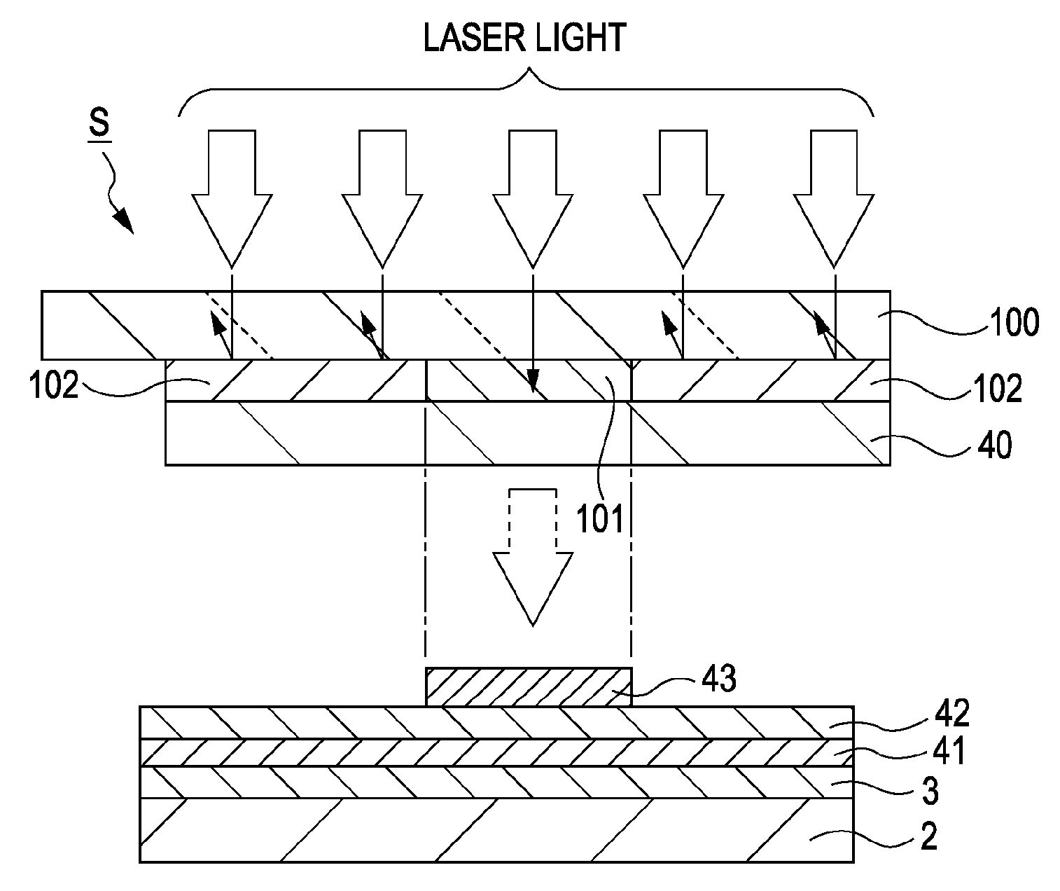
[0031] Furthermore, when an auxiliary wiring 7 is provided between the pixels a, the functional layer 4 above the auxiliary wiring 7 is removed so that the upper common electrode 5 and the auxiliary wiring 7 are brought into contact and connected with each other. By applying a voltage to the upper common electrode 5 using the auxiliary wiring 7, it is possib...


PUM

PropertyMeasurementUnit
Reflectanceaaaaaaaaaa
Thicknessaaaaaaaaaa

Abstract

A transfer substrate includes a support base which transmits laser light with a predetermined wavelength, a photothermal conversion layer provided on the support base, and a transfer layer provided on the photothermal conversion layer, the transfer layer including at least a luminescent layer. The photothermal conversion layer is composed of a first material and a second material having different absorptances with respect to the laser light.

Description

CROSS REFERENCES TO RELATED APPLICATIONS [0001] The present invention contains subject matter related to Japanese Patent Application JP 2005-128909 filed in the Japanese Patent Office on Apr. 27, 2005, the entire contents of which are incorporated herein by reference. BACKGROUND OF THE INVENTION [0002] 1. Field of the Invention [0003] The present invention relates to a luminescent material transfer substrate for transferring a transfer layer including at least a luminescent layer by sublimation to a target object, a method for fabricating a display device using the transfer substrate, and a display device fabricated using the transfer substrate. More particularly, the invention relates to a method for fabricating a display device that includes organic electroluminescent elements and a display device that includes organic electroluminescent elements. [0004] 2. Description of the Related Art [0005] Organic EL elements using electroluminescence (hereinafter referred to as “EL”) of orga...

Claims


Application Information

Patent Timeline
IPC IPC(8): H01L51/50H01L51/56B32B9/00
CPCH01L51/0013Y10T428/24802Y10S430/146H01L51/56C23C14/048Y10T428/31504H10K71/18H10K71/00
Inventor MATSUDA, EISUKENISHIGUCHI, MASAO
Owner JOLED INC
Why Eureka
Try Eureka