

Fabrication method of light emitting diode package
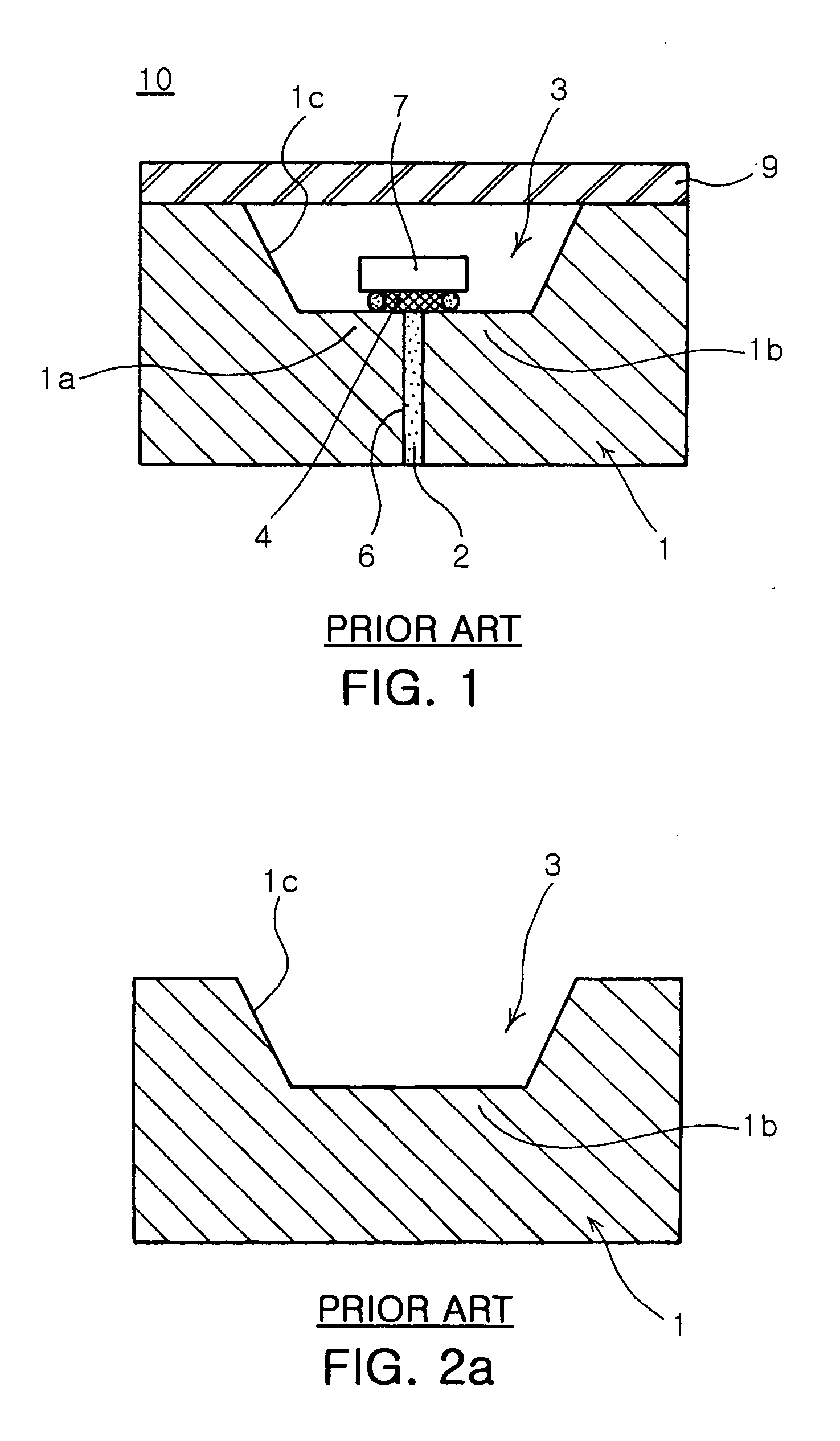
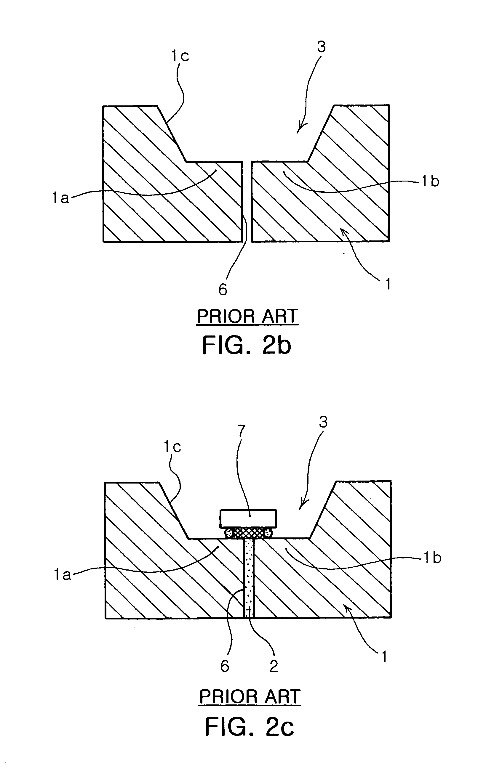
a technology of light-emitting diodes and fabrication methods, which is applied in the direction of basic electric elements, electrical apparatus, semiconductor devices, etc., can solve the problems of shortening the life of led devices, deteriorating led device properties, and no easy way to the narrow slot b>6/b> in the metal substrate, so as to achieve the effect of convenient application
- Summary
- Abstract
- Description
- Claims
- Application Information
AI Technical Summary
Benefits of technology
Problems solved by technology
Method used
Image

Examples
Embodiment Construction
[0034] Preferred embodiments of the present invention will now be described in detail with reference to the accompanying drawings. While the present invention will be shown and described in connection with the preferred embodiments, it will be apparent to those skilled in the art that modifications and variations can be made without departing from the spirit and scope of the invention as defined by the appended claims. The embodiments of the present invention are only aimed to provide a full explanation to a person having ordinary skill in the art. Therefore, the shape and size of the elements in the diagrams may be exaggerated for clearer explanation, with the same reference numerals designating the same elements throughout the drawings
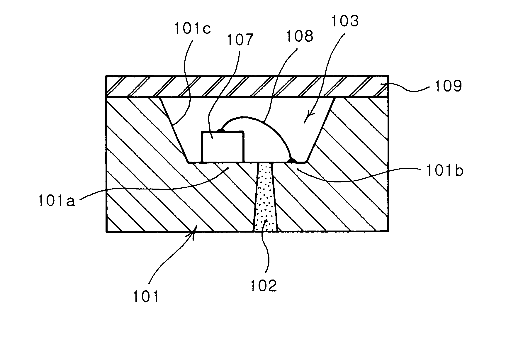
[0035]FIG. 3 is a cross-sectional view illustrating an LED package 100 fabricated according to an embodiment of the invention, and FIG. 4 is a plan view of the LED package 100 shown in FIG. 4. Referring to FIGS. 3 and 4, the LED package 100 includes...
PUM
 Abstract
Description
Claims
Application Information