Methods of fabricating semiconductor devices including contact plugs having laterally extending portions and related devices

a contact plug and lateral extension technology, applied in the field of semiconductor devices, can solve the problems of increasing the resistance of the pattern and/or the electrical short between the pattern, the contact plug may have a relatively complicated electrical connection structure, and the desired degree of integration may not be achieved, so as to reduce the probability of electrical failure, and reduce the resistance and ohmic characteristics

Active Publication Date: 2006-11-02
SAMSUNG ELECTRONICS CO LTD
View PDF13 Cites 21 Cited by
  • Summary
  • Abstract
  • Description
  • Claims
  • Application Information

AI Technical Summary

Benefits of technology

[0011] Some embodiments of the present invention may provide a contact plug having a relatively low resistance and an ohmic characteristic at an interface between the contact plug and a substrate and / or a single crystalline silicon layer pattern and a method of fabricating the same.
[0041] Thus, according to some embodiments of the present invention, a stacked semiconductor device may include a contact plug that has a relatively low resistance and ohmic characteristics at an interface between the contact plug and a substrate and at an interface between the contact plug and a single crystalline silicon layer pattern. As such, the stacked semiconductor device may have improved reliability and / or reduced probability of electrical failure. Additionally, a throughput of a process for manufacturing the stacked semiconductor device may be enhanced.

Problems solved by technology

As the patterns are reduced in size, however, several problems (such as increased resistance of the patterns and / or electrical shorts between patterns) may occur.
As such, a desired degree of integration may not be achieved by simply reducing the sizes of the patterns.
The contact plug may have a relatively complicated electrical connection structure between the transistors, and also may have a relatively low resistance and an ohmic characteristic.
However, as the contact plug is reduced in size and / or increased in height, the barrier metal layer may not be uniformly formed on the bottom surface and / or the sidewall of the contact hole.
Therefore, ohmic contact may not be properly provided at portions of the contact hole where the barrier metal layer is relatively thin and / or where the barrier metal layer is not formed.
However, when a barrier metal layer has poor step coverage, the barrier metal layer may not be uniformly formed between the source / drain regions and the contact plug.
Thus, ohmic contact also may not be provided between the contact plug and the source / drain regions, which may thereby cause electrical failure of the stacked semiconductor device.

Method used


Image

  • Methods of fabricating semiconductor devices including contact plugs having laterally extending portions and related devices
  • Methods of fabricating semiconductor devices including contact plugs having laterally extending portions and related devices
  • Methods of fabricating semiconductor devices including contact plugs having laterally extending portions and related devices

Examples


Embodiment Construction

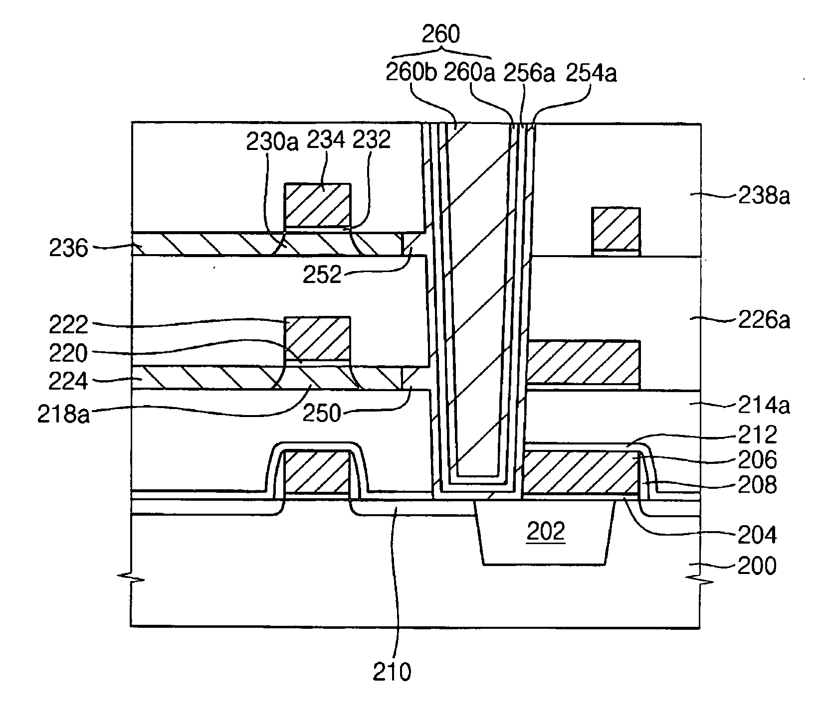
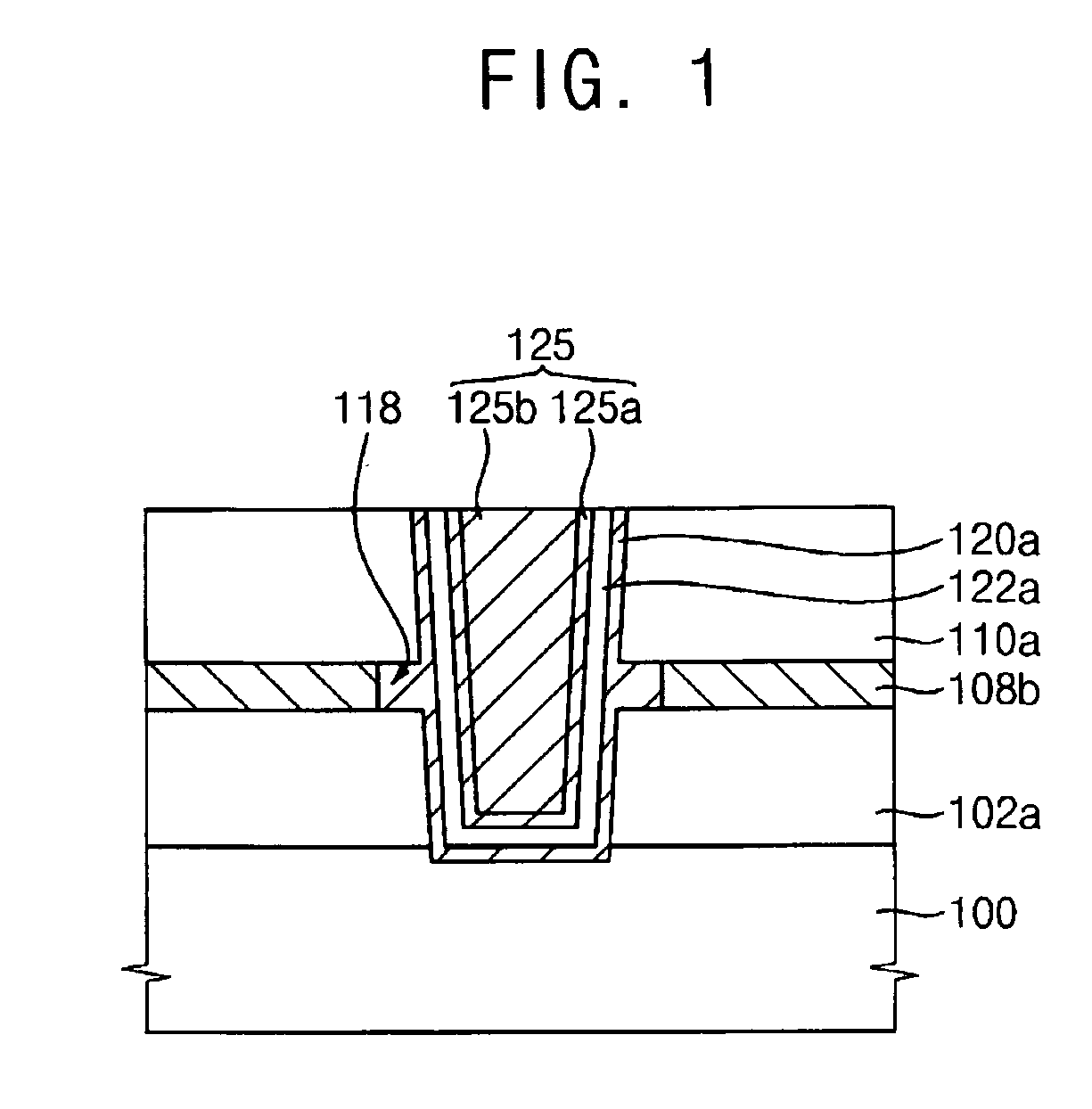
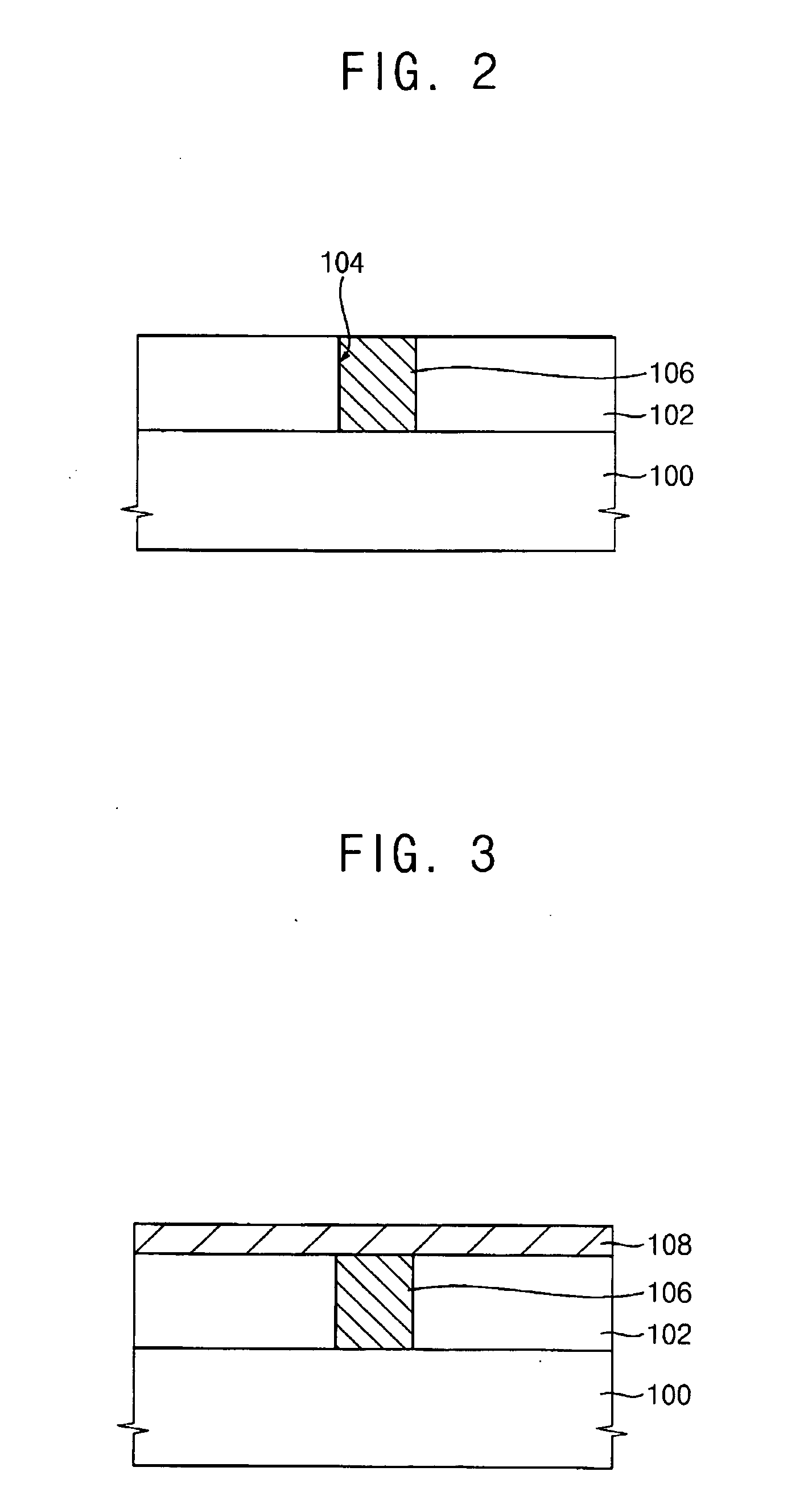
[0050] The present invention is described more fully hereinafter with reference to the accompanying drawings, in which embodiments of the present invention are shown. This invention may, however, be embodied in many different forms and should not be construed as limited to the embodiments set forth herein. Rather, these embodiments are provided so that this disclosure will be thorough and complete, and will fully convey the scope of the present invention to those skilled in the art. In the drawings, the sizes and relative sizes of layers and regions may be exaggerated for clarity. Like reference numerals refer to the same or similar elements throughout.

[0051] It will be understood that when an element or layer is referred to as being “on”, “connected to” or “coupled to” another element or layer, it can be directly on, connected or coupled to the other element, or layer or intervening elements or layers may be present. In contrast, when an element is referred to as being “directly o...


PUM


Abstract

In a method of forming an integrated circuit device, an opening is formed extending through a first and a second insulating layers and through a semiconductor layer therebetween to a surface of a substrate. The opening includes a recess in a sidewall thereof between the first and second insulating layers adjacent the semiconductor layer. A conductive plug is formed on the sidewall of the opening and on the surface of the substrate and laterally extending into the recess between the first and second insulating layers to contact the semiconductor layer. The semiconductor layer may be selectively etched at the sidewall without substantially etching the first and second insulating layers at the sidewall of the opening to form the recess between the first and second insulating layers. Related devices are also discussed.

Description

CROSS-REFERENCE TO RELATED APPLICATION [0001] This application claims priority under 35 U.S.C. § 119 from Korean Patent Application No. 2005-35018 filed on Apr. 27, 2005 in the Korean Intellectual Property Office, the disclosure of which is hereby incorporated by reference herein in its entirety. FIELD OF THE INVENTION [0002] The present invention relates to semiconductor devices, and more particularly, to methods of fabricating contact plugs and related devices. BACKGROUND OF THE INVENTION [0003] As semiconductor devices become highly integrated, sizes of patterns and intervals between the patterns may be greatly reduced. As the patterns are reduced in size, however, several problems (such as increased resistance of the patterns and / or electrical shorts between patterns) may occur. As such, a desired degree of integration may not be achieved by simply reducing the sizes of the patterns. Thus, stacked semiconductor devices have been developed. A stacked semiconductor device may incl...

Claims


Application Information

Patent Timeline
Patent Type & Authority Applications(United States)
IPC IPC(8): H01L21/4763H01L21/76
CPCH01L21/28562H01L21/76802H01L21/76843H01L27/1108H01L27/0688H01L27/11H01L21/76846H01L21/76898H10B10/125H10B10/00H01L21/3205
Inventor CHEONG, SEONG-HWEECHOI, GIL-HEYUNLEE, SANG-WOOPARK, JIN-HO
Owner SAMSUNG ELECTRONICS CO LTD
Why Eureka
Try Eureka