Rewriteable memory cell comprising a diode and a resistance-switching material

a resistance-switching material and memory cell technology, applied in digital storage, semiconductor devices, instruments, etc., can solve the problem of difficult to form a large, high-density array of such cells

Inactive Publication Date: 2006-11-09
SANDISK TECH LLC
View PDF34 Cites 683 Cited by
  • Summary
  • Abstract
  • Description
  • Claims
  • Application Information

AI Technical Summary

Problems solved by technology

It is very difficult to form a large, high-density array of such cells, however, due to the danger of disturbance between cells, high leakage currents, and myriad fabrication challenges.

Method used


Image

  • Rewriteable memory cell comprising a diode and a resistance-switching material
  • Rewriteable memory cell comprising a diode and a resistance-switching material
  • Rewriteable memory cell comprising a diode and a resistance-switching material

Examples


example

First Embodiment

[0060] A detailed example will be provided of fabrication of a monolithic three dimensional memory array formed according to a preferred embodiment of the present invention. For clarity many details, including steps, materials, and process conditions, will be included. It will be understood that this example is non-limiting, and that these details can be modified, omitted, or augmented while the results fall within the scope of the invention.

[0061] In general, the '470 application, the '549 application, the '824 application, and the '577 application teach memory arrays comprising memory cells, wherein each memory cell is a one-time programmable cell. The cell is formed in a high-resistance state, and, upon application of a programming voltage, is permanently converted to a low-resistance state. Specifically, teachings of the '470, '549, '824, '577 and other incorporated applications and patents may be relevant to formation of a memory according to the present inven...

second embodiment

cts, Above Diode

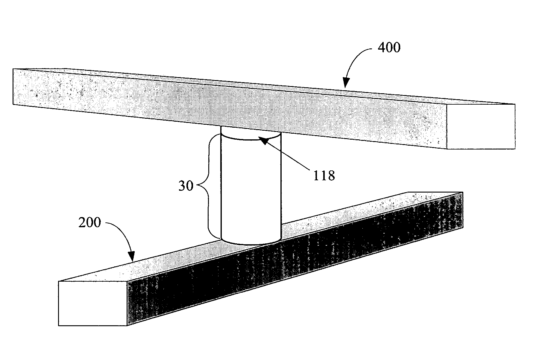
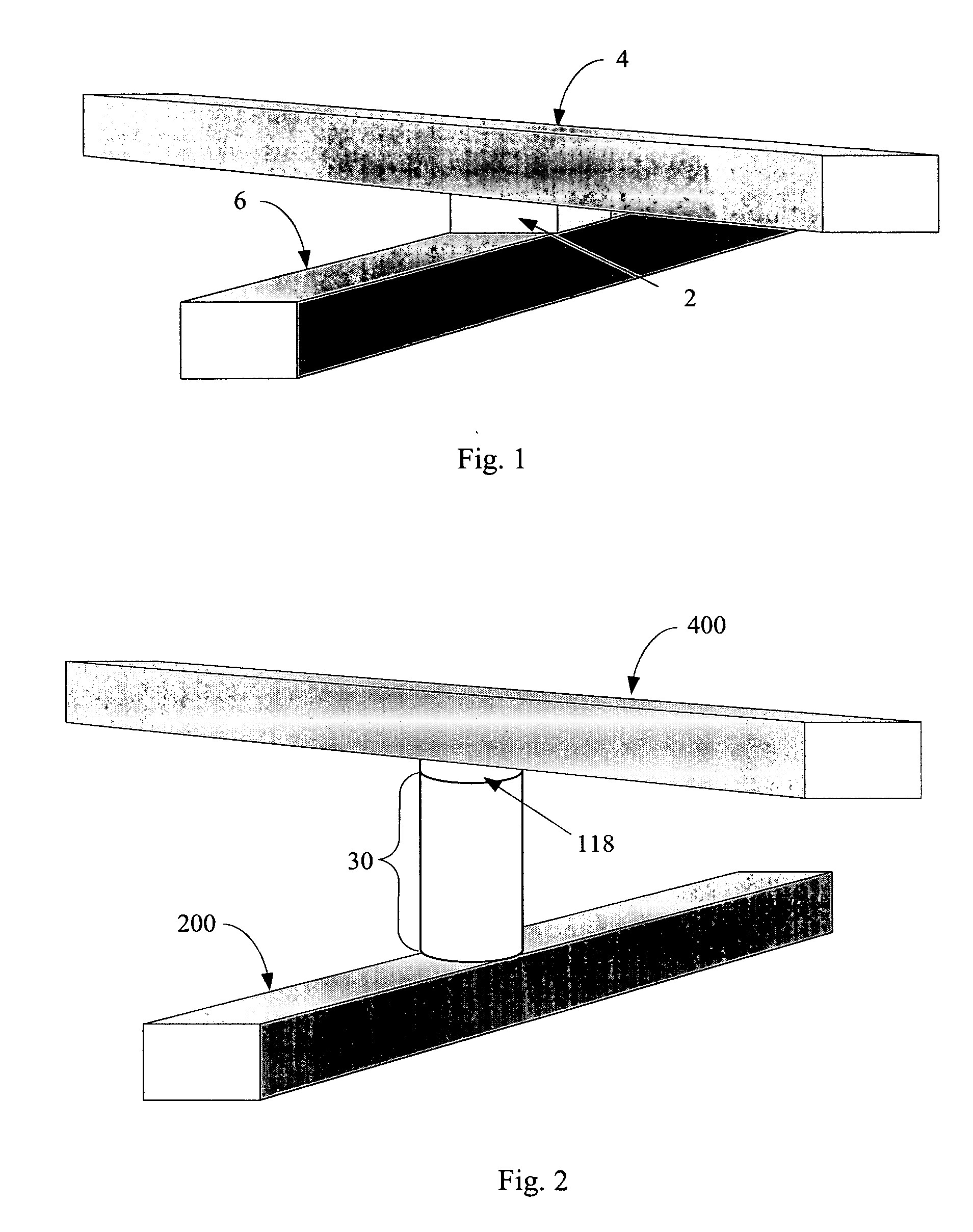
[0097]FIG. 10 showed an embodiment in which resistance-switching material 118 was sandwiched between noble metal layers 117 and 119. Preferred noble metals are Pt, Pd, Ir and Au. Layers 117 and 119 may be formed of the same noble metal, or of different metals.

[0098] When the resistance switching material is sandwiched between noble metal layers, the noble metal layers must be patterned and etched to assure that they do not provide unwanted conductive paths between adjacent diodes or conductors.

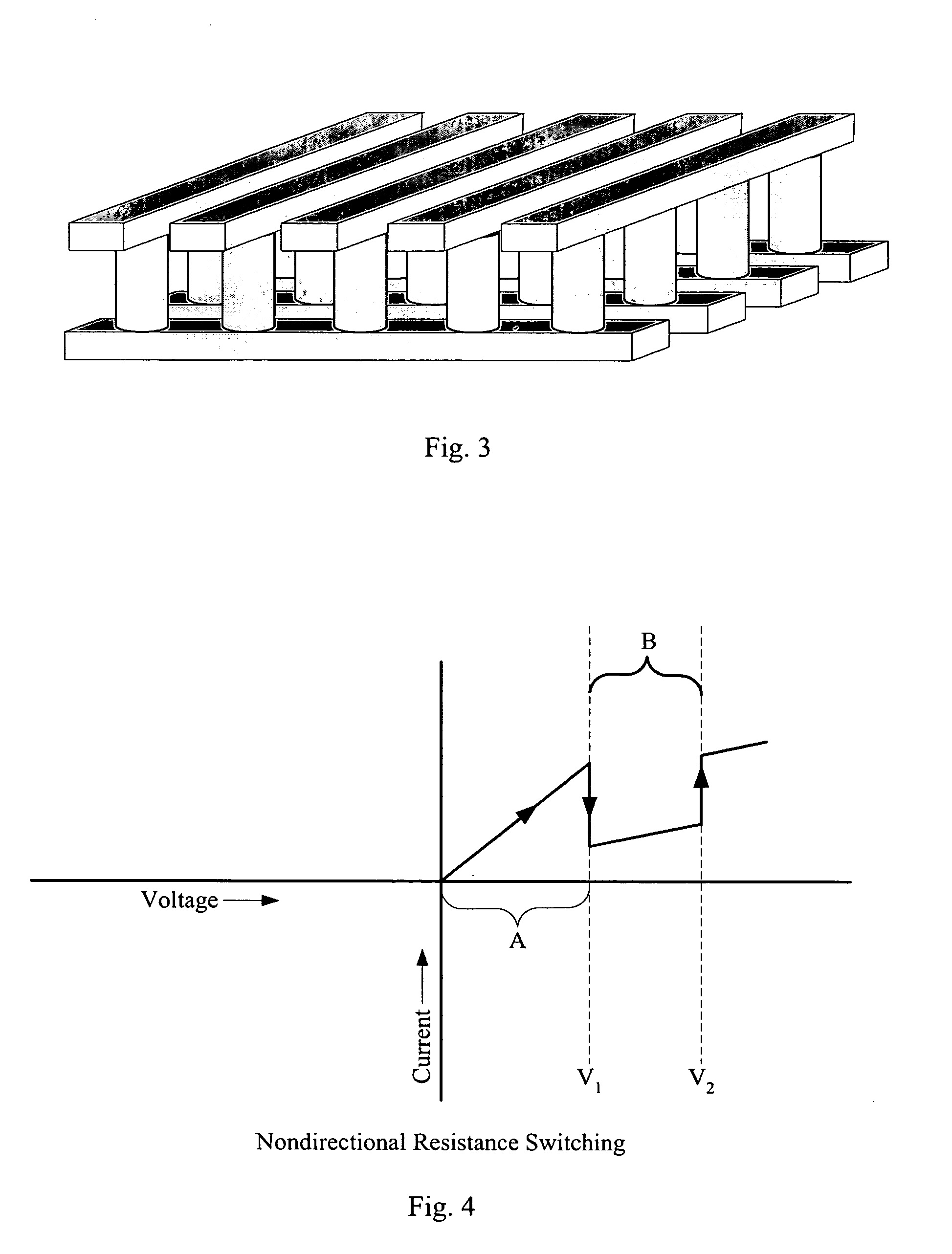
[0099] A memory level comprising cells like those of FIG. 10 is shown in cross-section in FIG. 13. In a preferred method to form this structure, bottom conductor 200 is formed as described earlier. Heavily doped germanium layer 112 and undoped germanium layer 114 are deposited as described earlier. In one preferred embodiment, the ion implantation of top heavily doped layer 116 can be performed on the blanket germanium layer before the pillars are patterned and etched. Next n...

third embodiment

acts, Below Diode

[0104] In an alternative embodiment, shown in FIG. 14, the resistance-switching elements 118, in this case sandwiched between noble metal layers 117 and 119, are formed below the diode, rather than above it.

[0105] To form this structure, bottom conductors 200 are formed as described earlier. Layers 117, 118, and 119 are deposited on the planarized surface 109 of conductors 200 separated by gap fill. The germanium stack, including heavily doped layer 112 and undoped layer 114, are deposited. Layers 114, 112, 119, 118, and optionally 117 are patterned and etched as described earlier to form pillars 300. After gap fill and planarization, top heavily doped region 116 is formed by ion implantation. Top conductors 400 are formed as in the previous embodiment, by depositing conductive layers, for example titanium nitride layer 120, aluminum layer 122, and titanium nitride layer 124, and patterning and etching to form the conductors 400.

[0106] As in other embodiments, if ...


PUM


Abstract

In a novel rewriteable nonvolatile memory cell formed above a substrate, a diode is paired with a reversible resistance-switching material, preferably a metal oxide or nitride such as, for example, NiO, Nb2O5, TiO2, HfO2, Al2O3, MgOx, CrO2, VO, BN, and AlN. In preferred embodiments, the diode is formed as a vertical pillar disposed between conductors. Multiple memory levels can be stacked to form a monolithic three dimensional memory array. In some embodiments, the diode comprises germanium or a germanium alloy, which can be deposited and crystallized at relatively low temperatures, allowing use of aluminum or copper in the conductors.

Description

RELATED APPLICATION [0001] This application is related to Herner et al., U.S. application Ser. No. ______, “High-Density Nonvolatile Memory Array Fabricated at Low Temperature Comprising Semiconductor Diodes,” (attorney docket number MA-145), hereinafter the ______ application, which is assigned to the assignee of the present invention, filed on even date herewith and hereby incorporated by reference in its entirety.BACKGROUND OF THE INVENTION [0002] The invention relates to a rewriteable nonvolatile memory array in which each cell comprises a diode and a resistance-switching element in series. [0003] Resistance-switching materials, which can reversibly be converted between a high-resistance state and a low-resistance state, are known. These two stable resistance states make such materials an attractive option for use in a rewriteable non-volatile memory array. It is very difficult to form a large, high-density array of such cells, however, due to the danger of disturbance between c...

Claims


Application Information

Patent Timeline
Patent Type & Authority Applications(United States)
IPC IPC(8): G11C11/00
CPCG11C11/5685G11C13/0007G11C13/0069G11C2013/009G11C2213/15H01L27/24G11C2213/34G11C2213/71G11C2213/72H01L27/101G11C2213/32H10B63/20H10B63/80H10N70/20H10N70/883H10N70/8833H10N70/826
Inventor HERNER, S. BRADPETTI, CHRISTOPHER J.
Owner SANDISK TECH LLC
Why Eureka
Try Eureka