Electroless deposition processes and compositions for forming interconnects

a technology of electroless deposition and interconnection, which is applied in the direction of liquid/solution decomposition chemical coating, coating, basic electric elements, etc., can solve the problems of affecting the device yield of the fabricated substrate, the displacement of voids from one layer to the next,

Inactive Publication Date: 2006-11-09
APPLIED MATERIALS INC
View PDF99 Cites 294 Cited by
  • Summary
  • Abstract
  • Description
  • Claims
  • Application Information

AI Technical Summary

Problems solved by technology

Defects, such as a seam or a void 114, may cause a series of problems during the fabrication of electronic devices depicted herein.
However, a more serious obstacle during fa

Method used


Image

  • Electroless deposition processes and compositions for forming interconnects
  • Electroless deposition processes and compositions for forming interconnects
  • Electroless deposition processes and compositions for forming interconnects

Examples


process example

Pretreatment Process Example

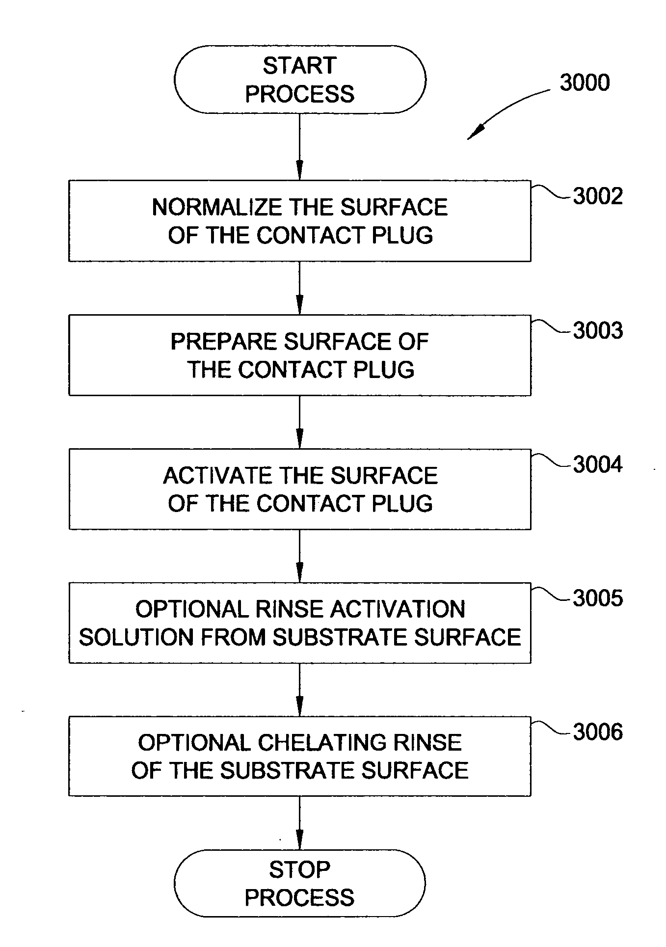
[0074] In one embodiment of the pretreatment process, various processing steps 3000 (see FIG. 6) are used to prepare the surface of the substrate prior to depositing the bulk fill layer 550. In one embodiment, the processing steps 3000 generally includes 1) an oxide removal step, 2) a surface preparation step, 3) an activation step, 4) an optional activation rinse step, and 5) an optional chelating rinse step. Each of the steps will be discussed in turn.

[0075] In the first step of the pretreatment process, or step 3002, the surface 512 is exposed to a clean solution to remove leftover etch residues from the formation of the interconnect feature 505 and / or any left over dielectric material (Item # 520FIG. 5B). In one aspect, the clean solution may be useful to remove some of the tungsten oxides formed on the surface 512, but cleaning solutions that are too aggressive will aggressively attack commonly used dielectric layer 520 materials. The preparation of...


PUM

PropertyMeasurementUnit
Molar densityaaaaaaaaaa

Abstract

In one embodiment, a method for depositing a material on a substrate is provided which includes positioning a substrate containing a contact within a process chamber, exposing the substrate to at least one pretreatment step and depositing a fill the contact vias by an electroless deposition process. The pretreatment step contains multiple processes for exposing the substrate to a wet-clean solution, a hydrogen fluoride solution, a tungstate solution, a palladium activation solution, an acidic rinse solution, a complexing agent solution or combinations thereof. Generally, the HARC via contains a tungsten oxide surface and the shallow contact via may contain a tungsten silicide surface. In some example, the substrate is pretreated such that both vias are filled at substantially the same time by a nickel-containing material through an electroless deposition process.

Description

CROSS-REFERENCE TO RELATED APPLICATIONS [0001] This application claims benefit of U.S. Provisional Patent Application Ser. No. 60 / 663,493, filed Mar. 18, 2005 [APPM 9916L], U.S. Provisional Patent Application Ser. No. 60 / 683,599, filed May 23, 2005 [APPM 9916L02], U.S. Provisional Patent Application Ser. No. 60 / 703,538, filed Jul. 29, 2005 [APPM 9916L03], U.S. Provisional Patent Application Ser. No. 60 / 703,633, filed Jul. 29, 2005 [APPM 9916L04], U.S. Provisional Patent Application Ser. No. 60 / 709,564, filed Aug. 19, 2005 [APPM 9916L05], and U.S. Provisional Patent Application Ser. No. 60 / 754,230, filed Dec. 27, 2005 [APPM 9916L06], which are all herein incorporated by reference.BACKGROUND OF THE INVENTION [0002] 1. Field of the Invention [0003] Embodiments of the invention generally relate to methods for depositing materials on substrates, and more specifically to methods of forming metal interconnects. [0004] 2. Description of the Related Art [0005] Multilevel, 45 nm node metalliz...

Claims


Application Information

Patent Timeline
IPC IPC(8): H01L21/4763H01L21/44
CPCB82Y30/00H01L23/53238C23C16/0281C23C16/045C23C16/14C23C18/1608C23C18/1651C23C18/1653C23C18/1678C23C18/31C23C18/32C23C18/34C23C18/38C23C18/40C23C18/48C25D5/34H01L21/02063H01L21/02074H01L21/28518H01L21/28556H01L21/288H01L21/2885H01L21/76814H01L21/76843H01L21/76844H01L21/76846H01L21/76847H01L21/76849H01L21/76855H01L21/76856H01L21/76861H01L21/76862H01L21/76874H01L21/76877H01L21/76879C23C16/0227H01L2924/0002H01L2924/00
Inventor ZHU, ZHIZEWEIDMAN, TIMOTHY W.STEWART, MICHAEL P.SHANMUGASUNDRAM, ARULKUMARKRISHNA, NETY M.KONECNI, ANTHONY
Owner APPLIED MATERIALS INC
Why Eureka
Try Eureka